This thread has been locked.

If you have a related question, please click the "Ask a related question" button in the top right corner. The newly created question will be automatically linked to this question.

ADS125H01: External Voltage Reference for ratiometric strain gauge measurement

Part Number: ADS125H01

Tool/software:

Dear Specialists,

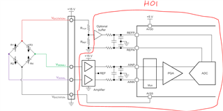
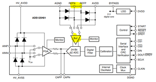
My customer is considering External Voltage Reference for ratiometric strain gauge measurement with ADS125H01.

External Voltage is 15V and current is 40mA.

According to the application note

https://www.ti.com/lit/an/sbaa532a/sbaa532a.pdf

+15V is feasible, but I don't know if 40mA of current can be passed through the ADS125H01.

Could you please advise?

If you have any external voltage reference for ratiometric strain gauge (ADS125H01 is preferable) ,could you please provide.

I appreciate your great help in advance.

Best regards,

Shinichi 

  • Hi Shinichi Inoue,

    I assume the circuit will be setup as shown in the image below, where the red box indicates all of the components inside the ADS125H01?

    If so, why would the ADC need to support 40mA? The 40mA is the current through the bridge, correct?

    -Bryan

  • Hi Bryan,

    Thank you for your reply.

    Yes, I believe that the customer would like to use 40 mA through the bridge circuit.

    You mean that 40 mA will not flow through AINP and AINN because the AINP and AINN of the ADS125H01 has high impedance (1Gohm min)?

    I appreciate your great help and cooperation.

    Best regards,

    Shinichi

  • Hi Shinichi Inoue,

    You mean that 40 mA will not flow through AINP and AINN because the AINP and AINN of the ADS125H01 has high impedance (1Gohm min)?

    Correct, the current is not going to flow into the ADC inputs due to high input impedance.

    -Bryan

  • Hi Bryan,

    Thank you for your reply.

    You mean that 40 mA will not flow through AINP and AINN because the AINP and AINN of the ADS125H01 has high impedance (1Gohm min)?

    Correct, the current is not going to flow into the ADC inputs due to high input impedance.

    I'll share this information with the customer.

    I appreciate your great help and cooperation.

    Best regards,

    Shinichi

  • Hi Bryan,

    The customer has an additional question.

    Could you please advise?

    ---

    According to the example design of the application note, there is a buffer after the reference divider as a option.

    What is the purpose?

    I think it is for reducing the current consumption of the reference divider.

    Is this correct?

    Could you please let me know the other purpose?

    ---

    I appreciate your great help and cooperation.

    Best regards,

    Shinichi

  • Hi Shinichi Inoue,

    Unbuffered reference inputs will look like a low impedance input to the reference pins, which means the reference source will be in parallel with a low impedance reference input. This will change the effective impedance of R_REF, leading to a gain error

    Note that the ADS125H01 has buffered reference inputs 

    -Bryan