This thread has been locked.

If you have a related question, please click the "Ask a related question" button in the top right corner. The newly created question will be automatically linked to this question.

ADS114S08B: Using Multiple ADS114S08B with Single SPI Bus in Multi-Channel Heating System

Part Number: ADS114S08B


Tool/software:

Hi,

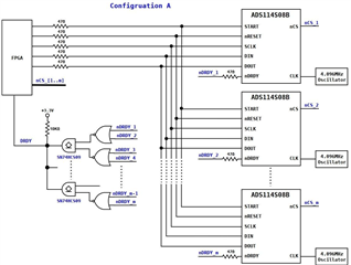
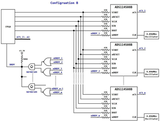
I am currently designing a multi-channel heating system that will utilize an FPGA to interface with multiple ADS114S08B devices for 4-wire RTD measurements. To optimize the number of FPGA signal lines, I plan to use a single SPI Bus to connect multiple ADS114S08B devices. I have a few questions regarding this setup:

    1. The datasheet (section 10.1.1) suggests placing a 47-ohm resistor in series with the digital input and output signals. Between the two resistor configurations shown in the attached diagram, which one is more suitable? Or is there a better connection method you would recommend?
    2. What is the maximum number of ADS114S08B devices that can be connected in parallel on the same SPI Bus?
    3. Does the choice of using an internal versus an external 4.096MHz clock signal affect the accuracy of the RTD resistance values obtained?
    4. In the attached diagram, the DRDY signal is connected such that after the FPGA sends the START/SYNC signal, can we ensure that all ADS114S08B devices have completed conversion and are ready for data readout simply by checking if DRDY = 1?

Thank you for your assistance.

Best regards,

  • Hi wjhsu,

    Answers to your questions:

    The datasheet (section 10.1.1) suggests placing a 47-ohm resistor in series with the digital input and output signals. Between the two resistor configurations shown in the attached diagram, which one is more suitable? Or is there a better connection method you would recommend?

    In general these resistors should be placed near the signal driver. For example, the controller drives the DIN pin, so the resistor would be near that pin on the controller; comparatively, the ADC drives the DOUT pin, so the resistor should be near that pin on the ADC. However, this is not super important at these relatively low communication frequencies

    What is the maximum number of ADS114S08B devices that can be connected in parallel on the same SPI Bus?

    This depends on the speed you are running at and the total capacitance on the bus (which includes the capacitive load of each device + layout / trace capacitance). So there is no single answer to this question, but you would need to tradeoff between those two parameters. The slower the speed, the more devices you can place on the bus.

    Does the choice of using an internal versus an external 4.096MHz clock signal affect the accuracy of the RTD resistance values obtained?

    Not directly. If you are using the digital filter to reject certain frequencies e.g. 50/60Hz, then the accuracy of the oscillator affects how much rejection you would get. But the clock frequency doesn't change the intrinsic measurement accuracy, and these input frequencies are too low to care about clock jitter

    In the attached diagram, the DRDY signal is connected such that after the FPGA sends the START/SYNC signal, can we ensure that all ADS114S08B devices have completed conversion and are ready for data readout simply by checking if DRDY = 1?

    You probably don't need all of that extra circuitry. In reality, if you issue the START/SYNC signal each time, you know how long it will be until data is available, within the tolerance of your clock of course. So let's say data will be ready in 1 ms based on your selected data rate, and your clock accuracy is 2% max. That is 1.02ms, so if you wait 1.1 ms for some additional margin, you can be sure all of the ADCs have completed the conversion process.

    Are you going to issue START/SYNC each time you want a conversion? Or just once at the beginning and then take continuous data from each ADC after that?

    -Bryan

  • Hi Bryan,

    Thank you for your detailed response to my questions. As we are still in the circuit design phase, we have not yet decided whether to use continuous or single-shot conversion mode. We will consider your suggestion of ensuring ADC conversion completion by delaying a specific time after sending the START/SYNC signal during the firmware design stage.

    Thank you again for your assistance.

    Best regards,