This thread has been locked.
If you have a related question, please click the "Ask a related question" button in the top right corner. The newly created question will be automatically linked to this question.
Tool/software:
Hello everyone, how are you?
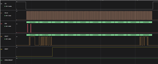
I have a few questions regarding the configuration and data reading of the ADS131M08. I've been working with this ADC for a short time and have encountered some difficulties. I believe I’ve correctly configured the ADC for continuous reading, but I can't see any variation in the values (in bits on the oscilloscope), even when altering the analog input value.
I’m using an ST microcontroller and so far I've been able to write to registers and read them back to verify the writing. I managed to reset it via command, but not via pin. Now I want to perform continuous data reading. I’m changing the analog input value and monitoring the SPI communication with an oscilloscope, but the frame corresponding to the analog reading value does not change.
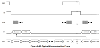
I’ve configured the program to read only on AI1, and the SPI word sent by the ADC is made up of 10 frames, where frames 3 to 10 are the analog inputs, and I don’t know what the first two frames represent. Could you help me?
void reset_ads (void) { HAL_SPI_Transmit(&hspi3, reset, 3, 100); int i = 0; int num_repeticoes = 9; while (i < num_repeticoes) { HAL_SPI_Receive(&hspi3, data_readed, 3, 100); data_readed[0] = 0b00000000; data_readed[1] = 0b00000000; data_readed[2] = 0b00000000; i++; } } void standby (void) { uint8_t standby [3]; standby [0] = 0b00000000; standby [1] = 0b00100010; standby [2] = 0b00000000; HAL_SPI_Transmit (&hspi3, standby, 3, 100); } int main(void) { HAL_Init(); SystemClock_Config(); MX_GPIO_Init(); MX_USART2_UART_Init(); MX_SPI3_Init(); MX_UART4_Init(); MX_UART5_Init(); pre_data [0] = 0b10100001; pre_data [1] = 0b10000000; pre_data [2] = 0b00000000; data_readed [0] = 0b00000000; data_readed [1] = 0b00000000; data_readed [2] = 0b00000000; reset [0] = 0b00000000; reset [1] = 0b00010001; reset [2] = 0b00000000; wrdata[0] = 0b01100001; wrdata[1] = 0b10000000; wrdata[2] = 0b00000000; clkreg [0] = 0b00000010; clkreg [1] = 0b01001110; clkreg [2] = 0b00000000; //-------------------- reset_ads(); HAL_Delay(1); //STAND-BY HAL_GPIO_WritePin (CS_ADS131M08_GPIO_Port, CS_ADS131M08_Pin, GPIO_PIN_RESET); standby(); HAL_Delay(1); HAL_GPIO_WritePin (CS_ADS131M08_GPIO_Port, CS_ADS131M08_Pin, GPIO_PIN_SET); //CONFIGURAÇÃO DOS CANAIS DE LEITURA DO ADC EM 03H HAL_GPIO_WritePin (CS_ADS131M08_GPIO_Port, CS_ADS131M08_Pin, GPIO_PIN_RESET); HAL_SPI_Transmit (&hspi3, wrdata, 3, 100); //WRITE IN 03H asm("nop"); HAL_SPI_Transmit (&hspi3, clkreg, 3, 100); //DATA 03H HAL_GPIO_WritePin (CS_ADS131M08_GPIO_Port, CS_ADS131M08_Pin, GPIO_PIN_SET); //WAKEUP ADC HAL_GPIO_WritePin (CS_ADS131M08_GPIO_Port, CS_ADS131M08_Pin, GPIO_PIN_RESET); HAL_SPI_Transmit (&hspi3, wakeup, 3, 100); //COMANDO WAKEUP HAL_GPIO_WritePin (CS_ADS131M08_GPIO_Port, CS_ADS131M08_Pin, GPIO_PIN_SET); HAL_GPIO_WritePin (CS_ADS131M08_GPIO_Port, CS_ADS131M08_Pin, GPIO_PIN_RESET); data_readed [0] = 0b00000000; data_readed [1] = 0b00000000; data_readed [2] = 0b00000000; while (1) { int i = 0; int num_repeticoes = 10; while (i < num_repeticoes) { HAL_SPI_Receive(&hspi3, data_readed, 3, 100); data_readed[0] = 0b00000000; data_readed[1] = 0b00000000; data_readed[2] = 0b00000000; i++; } } }
Hi Felipe de Andrade,
Welcome to the E2E forum. Were you trying to say you received 10 words (24-bit per word) for each frame? If so, the first word is status word, word 2-9 are channel data, the last word should be CRC, please see the typical timing frame on ADS131M08 below:
Can you check the voltage on REFIN? It seems like you are using a while loop but not checking /DRDY signal to retrieve the data, please confirm. Can you provide your timing plot like the timing I just showed above? Did you tie the /SYNC/RESET pin to high(DVDD)?
BR,
Dale
Hello, Dale
Yes, I received 10 words of 24 bits per frame. However, shortly after sending the message here on the forum, I realized that I was able to read the analog input, but the input signal was higher than my reference signal, so the value was getting saturated. At the moment, I am adjusting the voltage between 0 and 1.25V on Channel 1 of the ADC.
In the image above, the two larger dark blue signals are the DRDY pulse. Between these pulses, I have a frame with 10 words of 24 bits (yellow is the clock, and light blue is the MISO). In the programming, I configured the 03H register (clock register) by sending the command 0b00000010 01001110 00000000, where I fill in with 8 zeros at the end just to complete the 24 bits (is this correct?). According to the datasheet, this command configures Channel 1 as enabled and the other channels as disabled. So, analyzing the 10 words received on the oscilloscope, I have: (STATUS - ???? - CH0 - CH1 - CH2 - CH3 - CH4 - CH5 - CH6 - CH7), where only CH1 has a reading because it is the only one enabled. I would like to know what this second word is, because if I enable CH0, it is the third word that receives a signal.
The SYNC/RESET pin is at a high level, and my reference is at 1.25V.
Best regards,
Felipe.
Hi Felipe de Andrade,
Filling in with 8 extra zeros at the end of the command to implement the 24-bit word is correct, but the command '0b00000010 01001110 00000000' you sent to the ADC is not a valid command to write the 03h CLOCK register, the correct command is 0x61 80 00 + register data. Below is the timing example to write the CLOCK register with 0x0F0E data. Note that this timing was captured on ADS131M04 that has the same timing as ADS131M08 but it only has 4 input channels. You can check the Table 8-11. Command Definitions and also the timing in Figure 8-25 in ADS131M08 datasheet. Therefore, your command actually did not program the CLOCK register and did not disable the channels. The timing you showed is the correct response from the ADS131M08 device.
BR,
Dale
Good morning, Dale!
You may not have noticed, but I am sending the command to write to the 03H register before sending the value I want to save in 03H. This is described in the program in the first message I sent.
wrdata[0] = 0b01100001; wrdata[1] = 0b10000000; wrdata[2] = 0b00000000; clkreg [0] = 0b00000010; clkreg [1] = 0b01001110; clkreg [2] = 0b00000000; //03H REG CONFIGURATION HAL_GPIO_WritePin (CS_ADS131M08_GPIO_Port, CS_ADS131M08_Pin, GPIO_PIN_RESET); HAL_SPI_Transmit (&hspi3, wrdata, 3, 100); //WRITE COMMAND 03H asm("nop"); HAL_SPI_Transmit (&hspi3, clkreg, 3, 100); //DATA 03H HAL_GPIO_WritePin (CS_ADS131M08_GPIO_Port, CS_ADS131M08_Pin, GPIO_PIN_SET);
The forum link shown below also demonstrates how this operation is done:
The only difference is that for the write command, I don't give a pulse on CS; I just wait for a period using the (asm("nop")) command as shown in the link above. But for testing, I re-uploaded the program to the MCU and got the same result that I sent in the previous response.
BR,
Felipe.
Hi Felipe,
Thank you for pointing it out. Are you ting the /CS to GND directly? If so, you need to send all SCLKs or words in each frame because the ADS131M0x ADC determines the end and start of the frame by counting the number of SCLKs without /CS signal. Did you read the CLOCK register back to check if your WREG command has successfully written your data to the register? If you could capture your timing ( first two frames as you mentioned) with a logic analyzer like the timing I showed above, I can take a close look at it.
BR,
Dale
Hello, Dale! I am not connecting the CS pin directly to GND. It is connected to a digital pin of the MCU. I checked in the CLOCK register to see if the command I sent is being saved, and everything is OK. In the image below, I demonstrate this:
In the first 24-bit frame, I send the write command to register 03H (01100001 10000000 00000000), and after that, I send the content I want to save in 03H (00000110 01001110 00000000). After completing these steps, I sent a read command to register 03H (10100001 10000000 00000000) and provided a variable to collect the data in 03H, obtaining what was previously recorded (00000110 01001110 00000000). In the images, the yellow line represents the Clock, the purple one is MOSI, and the blue one is MISO.
BR,
Felipe.
Hi Felipe de Andrade,
Dale is out of the office right now - can you let me know what the issue is at this point?
It seems like the issue reading data has been resolved (the input was larger than the reference voltage), and now you are reading and writing registers correctly (the previous post shows this for the CLOCK register). So I am unclear what your issue is
-Bryan
Hello, Bryan!
Sorry for the delay; the last few days have been quite hectic. My problem now is understanding what each word in the frame that the ADC sends me means, as I questioned in the first response I gave to Dale. I will post it again here:
"In the image above, the two larger dark blue signals are the DRDY pulse. Between these pulses, I have a frame with 10 words of 24 bits (yellow is the clock, and light blue is the MISO). In the programming, I configured the 03H register (clock register) by sending the command 0b00000010 01001110 00000000, where I fill in with 8 zeros at the end just to complete the 24 bits (is this correct?). According to the datasheet, this command configures Channel 1 as enabled and the other channels as disabled. So, analyzing the 10 words received on the oscilloscope, I have: (STATUS - ???? - CH0 - CH1 - CH2 - CH3 - CH4 - CH5 - CH6 - CH7), where only CH1 has a reading because it is the only one enabled. I would like to know what this second word is, because if I enable CH0, it is the third word that receives a signal."
BR,
Felipe.
Hi Felipe de Andrade,
I tried recreating your code, see below. I am sending the exact settings you have that write to REG 0x03 to turn off all channels except ch0
I applied -0.5V to ch0, and you can see that the hex value I received corresponds to -0.5V assuming VREF = 1.2V and gain = 1
You can also see from the second image that the CRC calculation is correct
Are you absolutely sure that the third word in your frame corresponds to ch0?
-Bryan
Good morning, Bryan.
I was analyzing and modifying the code yesterday and noticed something. I wrote in my while loop to receive the data in 12 words, with the ADC delivering the STATUS register and the 8 channels, totaling 9 words. The ADC duplicated the remaining 3 words from the beginning of my frame, delivering the STATUS register again, along with channel 0 and channel 1, totaling 12 words.
In the example in the image below, I was collecting a total of 10 words, but my CRC is disabled, so my ADC only delivered 9 words in my frame. The first word delivered after the pulse on CS is just garbage replicated from CH1, as it changes together when I vary the input voltage of Channel 1. If I ignore it, I have exactly the STATUS register as the first word and the 8 channels following it, completing the frame.
BR,
Felipe.
Hi Felipe de Andrade,
I have been out of the office for the last two weeks, thanks for your patience
Is your issue resolved then? It seems like you were clocking out the wrong number of words, leading the issue where the data was not where you expected it to be. And now that you have identified that issue, it has been fixed. Is that correct?
-Bryan