This thread has been locked.

If you have a related question, please click the "Ask a related question" button in the top right corner. The newly created question will be automatically linked to this question.

DAC8830: Consultation on abnormal noise issues

Part Number: DAC8830
Other Parts Discussed in Thread: OPA388

Tool/software:

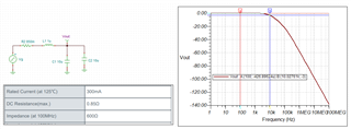
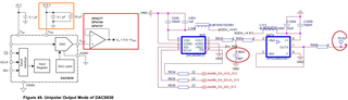
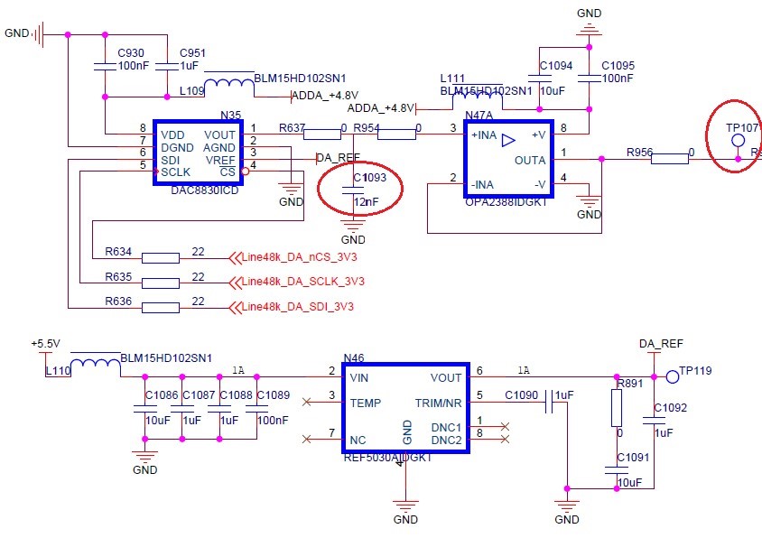
I have chosen the DAC8830 to realize the output of analog signals ranging from 200Hz to 48kHz. The sampling rate is 153.6kHz. The circuit is designed according to the circuit diagram provided in the official website's document TIDA01402. The actual circuit is shown in the following figure.

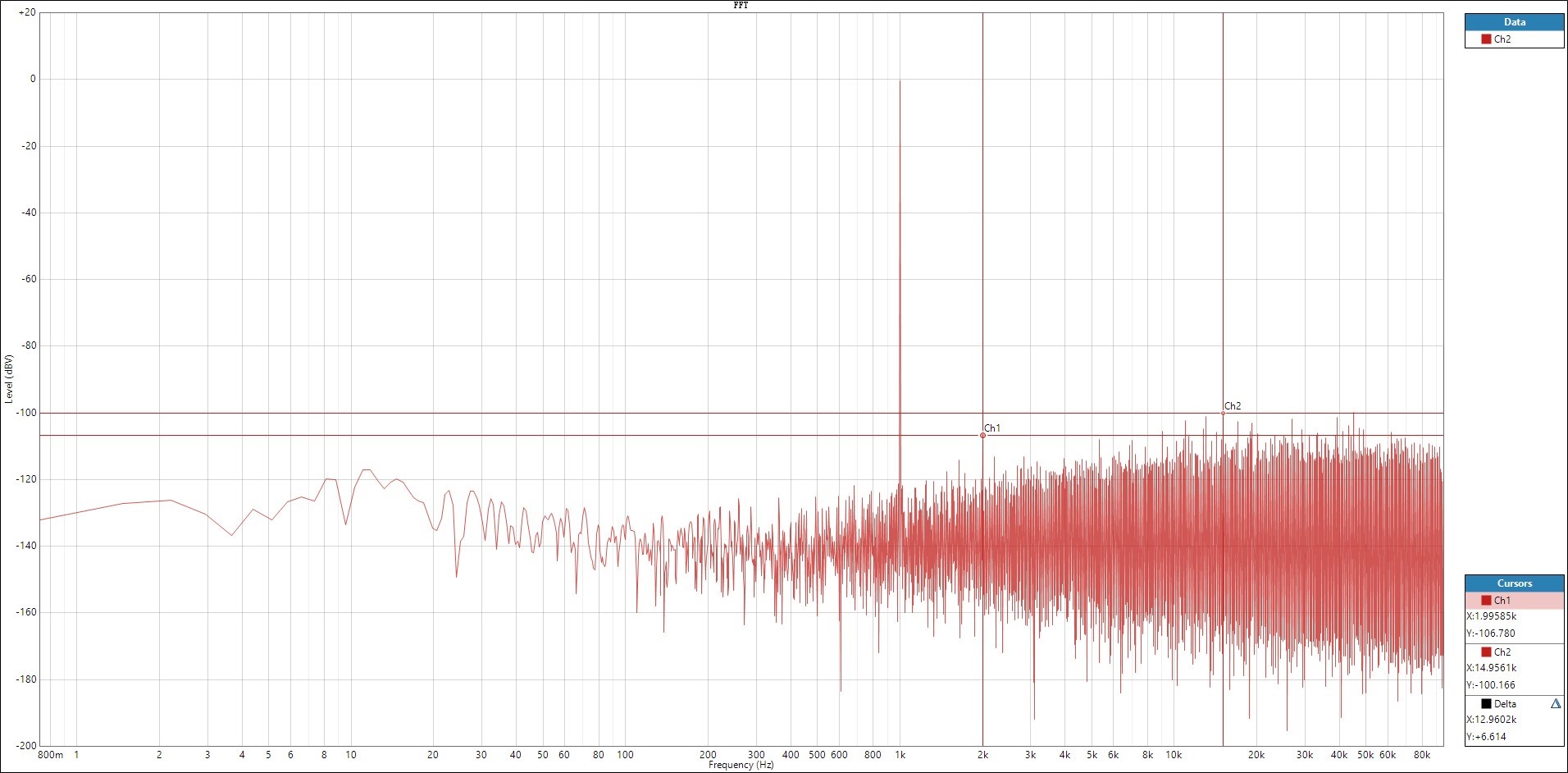
When testing the circuit, I use the IP core on the FPGA platform to generate a sinusoidal digital sequence having a frequency of 1 kHz and an amplitude of 1 Vrms. This signal is then sent to the DAC8830. I measure the analog signal at test point TP107 (with the latter stage circuit disconnected). The measured output signal spectrum is shown in the following figure. The noise floor is basically below -100 dBV. The signal quality is acceptable.

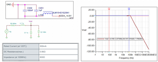
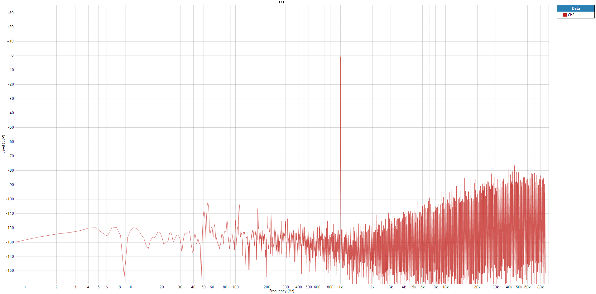
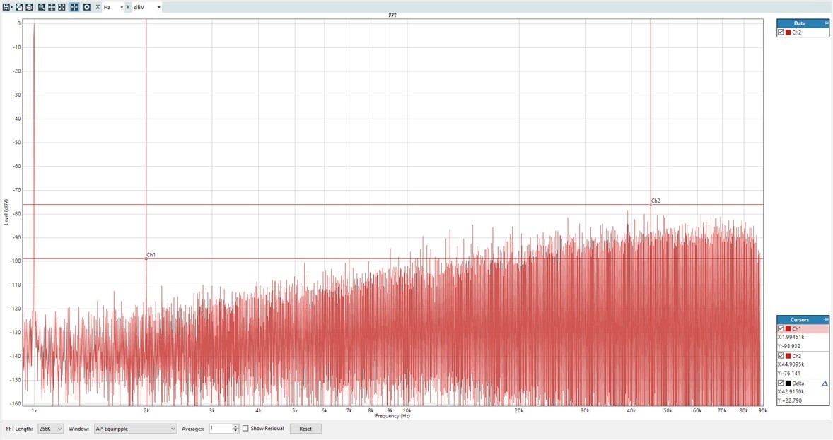
However, since the signal bandwidth reaches 48 kHz, the capacitance value of C1093 in the circuit must be adjusted. In the circuit of TIDA01402 document, a capacitance value of 12 nF is selected. According to the output impedance of 6.25 kΩ given in the DAC8830 datasheet, the cut-off frequency should be about 2.1 kHz, which cannot meet the usage requirements. Changing the capacitance value of C1093 to 340 pF results in a cut-off frequency of about 75 kHz. After changing the capacitance value, a sinusoidal digital sequence having a frequency of 1 kHz and an amplitude of 1 Vrms is still used as the test signal. The signal spectrum measured at TP107 is shown as follows. As the frequency increases, the noise floor also rises. The highest noise floor within the Nyquist frequency reaches 80 dBV. This is rather different from the noise specification of 10 nV/√Hz as described in the datasheet.

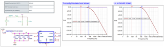
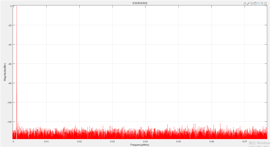
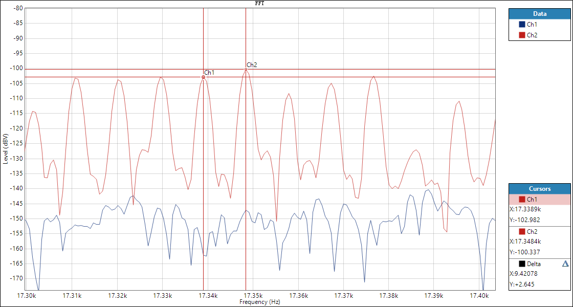
I had suspected that the signal noise might be related to the noise of the reference voltage or power supply. So, I attempted to add filtering treatment to the VREF pin of the DAC8830. However, I discovered that even after reducing the noise on this pin, there was no improvement in the noise of the output signal, as shown in the following figures. Similar tests were performed on the VDD pin, and the results were similar.

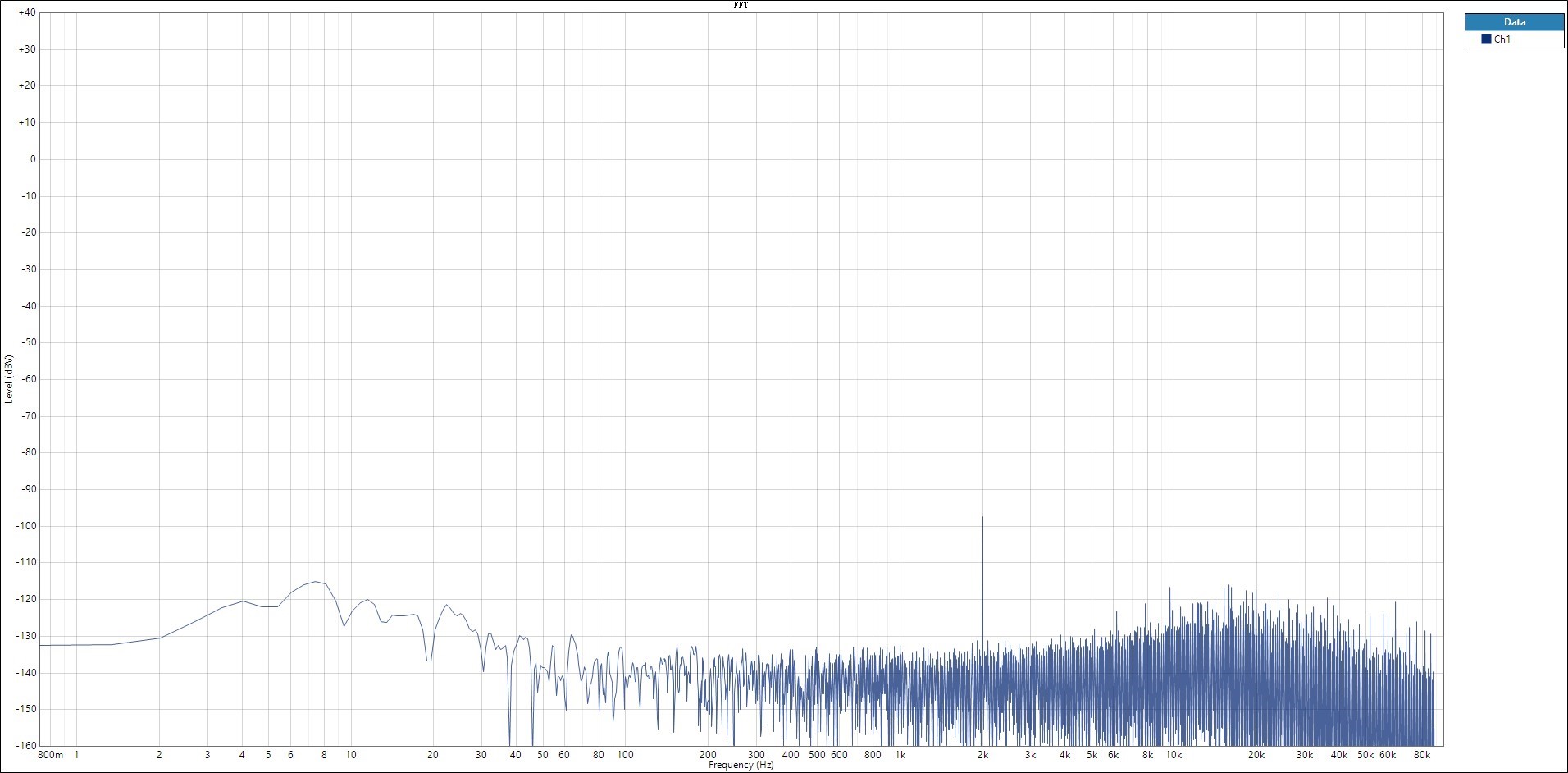
                           Figure:Noise level of VREF pin before adding filtering

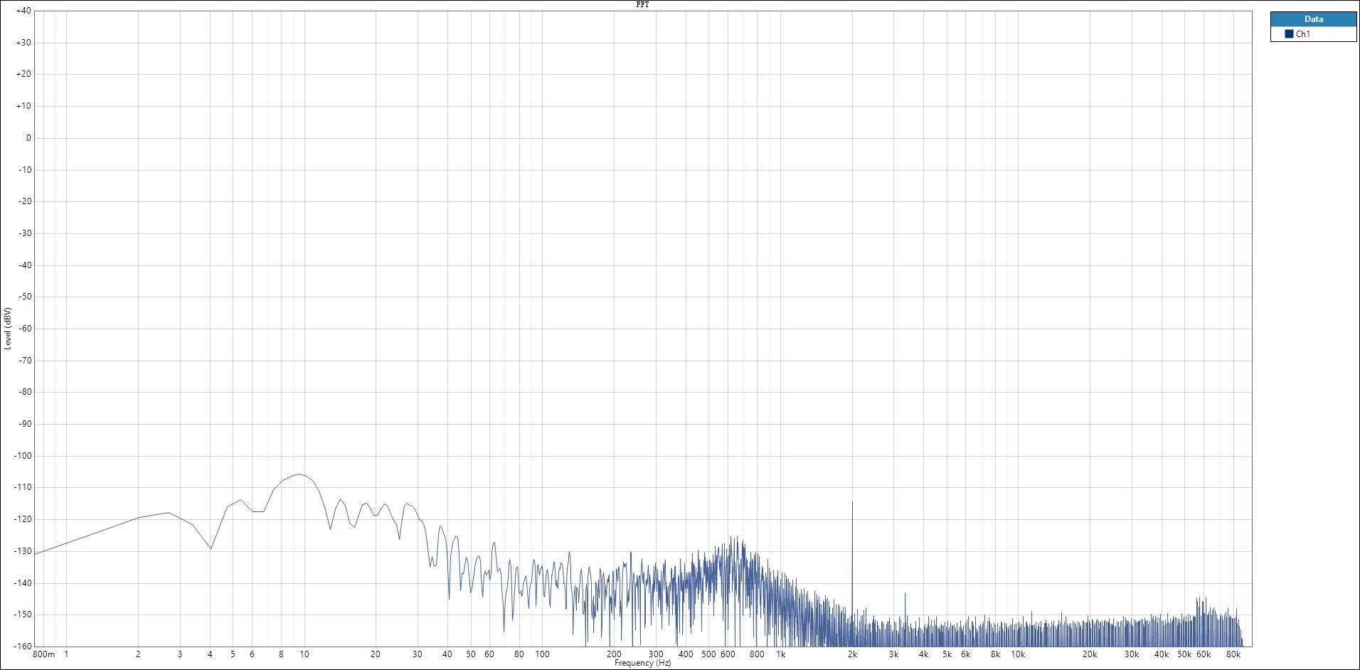
                            Figure:Noise level of VREF pin after adding filtering

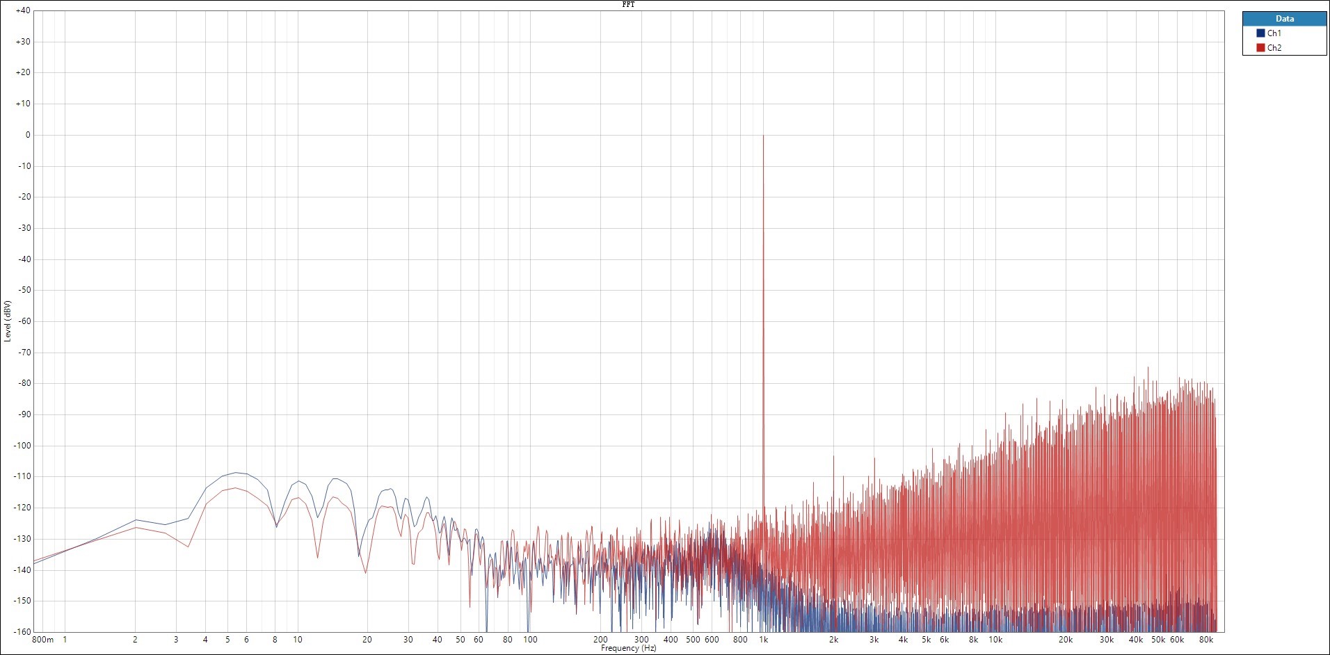
             Figure:The optimization of noise on the VREF pin has no effect on signal noise

This noise floor level is definitely not what the DAC8830 is supposed to be. Hence, I'd like to post a query to seek advice on what might be the cause for the degradation of the noise level.

Besides,If there are relevant literatures, I would greatly appreciate recommendations.

Thanks,

Howie

  • Hi Howie, 

    discovered that even after reducing the noise on this pin, there was no improvement in the noise of the output signal, as shown in the following figures. Similar tests were performed on the VDD pin, and the results were similar.

    You are likely using switching power supply to generate 5.5Vdc. Please let me know what is the switching frequency of your power supply. 

    At OPA388, the frequency pole is at approx. 21kHz. I would move the pole to 5kHz range, or no greater than 10kHz. Please use low ESR caps. With 2X low ESR 10uF capacitors in parallel with the ferrite chip, the pole should be placed at 10kHz. 

    BLM15HD102SN1 600ohm 100MHz Ferrite Chip 08162024.TSC

    In the image below above the DAC, copy the LC filter from OPA388 supply rails. In this one, there is Q generated near the cutoff frequency, which it should be avoided.  

    In your voltage reference, I would place the low frequency pole at approx. 5-6kHz range, and you would have -40dB/dec attenuation or roll off afterwards. It should improve your noise situation (rising as frequency increases).  Please make sure that you are taking care of your layout, don't share the switching GND from switching power supply with your analog GND; and terminate all the GND plane in a single point, which it should be tied and terminated to your metal chassis/earth GND. 

    BLM15HD102SN1 600ohm 100MHz Ferrite Chip 32uF 08162024.TSC

    Regarding to OPA388, this is just a buffer. What is load after TP107? Please make sure that OPA388 is not driving capacitive load. If it does, it requires additional loop compensation. 

    For OPA388, please try the following. Please matching the input and feedback resistor (even though this is buffer, because OPA388 is chopper amplifier). Please another LPF before TP107, and this will attenuate the undesired high frequency noise from TP107.


    OPA2388 08162024.TSC

    Please let me know if this helps. 

    Best,

    Raymond

  • Hi Raymond,

    I am very grateful for your attention to my question and the reply you gave.

    •The 5.5Vdc power supply is directly provided by an external DC power supply unit. I have attempted to replace the external power supply, but the noise phenomenon persists.

    •I attempted to disconnect the OPA388 and measure the output of DAC8830 directly. The test point is C1093 as shown in the schematic. R954 is left unconnected. The noise spectrum is largely identical to the above figure. That is, when the signal comes out from DAC8830, noise already exists, and it should be unrelated to the buffer section.

    •Regarding the filter circuits for the reference voltage and the DAC power supply voltage, adjustments have been made according to your suggestion. However, they have had no impact on the noise.

    •Regarding concerns about PCB layout, I have also tried to connect the SPI interface of the FPGA to a DAC8830 development board purchased online using jumper wires. The signal output from the DAC8830 on the development board has the same noise issue. This should lead us to conclude that this noise is not related to PCB layout. This test makes me suspect whether there is a problem with the signal source itself. However, when I collect the data source output from the FPGA using a logic analyzer, the obtained data source spectrum is good, as shown in the following figure.

    •There is a discovery: When magnifying the time axis of the noise spectrum for observation, it is found that the noise is not random noise but fixed noise with an interval of approximately 10Hz, as shown in the following figure(red line). However, there is no circuit on my board that operates at a frequency of 10Hz.

    As of now, the noise issue remains unresolved. I am looking forward to get support again.

    Thank you!

    Best,

    Howie

  • Hi Howie,

    If the noise is generated from DAC8830, it will be the best to get help from our DAC team. I do not support this product line. However, DAC is recommended to be buffer directly. It is unlikely that it is able to drive 12nF capacitor directly. 

    The initial noise plots are shown the issues are high frequency and increasing. The current noise is 10Hz range. If it was 10Hz range, it should not show up in the high frequency plot. Are you using switching power supply that regulating +5.5Vdc supply? With the uses of ferrite components, my guess is that you had a noisy rail from the 5.5Vdc regulator. 

    I do not know where 10Hz from without knowing your circuit better. It could be from the power supply fluctuation. You need to tell me more about your operating environment. It could also be picked up or coupled from the external test equipment (EMI). 

    Best,

    Raymond