This thread has been locked.

If you have a related question, please click the "Ask a related question" button in the top right corner. The newly created question will be automatically linked to this question.

ADS8686S: SPI communication via SDOA returning garbage

Part Number: ADS8686S
Other Parts Discussed in Thread: ADS8681, DP83640

Tool/software:

I am using the ADS8686S in software serial mode with 1-wire data output, SDOA only.

I am interfacing with a STM32H723ZGT6 as Full-duplex master using these SPI settings:

  hspi1.Instance = SPI1;
  hspi1.Init.Mode = SPI_MODE_MASTER;
  hspi1.Init.Direction = SPI_DIRECTION_2LINES;
  hspi1.Init.DataSize = SPI_DATASIZE_8BIT;
  hspi1.Init.CLKPolarity = SPI_POLARITY_HIGH;
  hspi1.Init.CLKPhase = SPI_PHASE_1EDGE;
  hspi1.Init.NSS = SPI_NSS_SOFT;
  hspi1.Init.BaudRatePrescaler = SPI_BAUDRATEPRESCALER_2;
  hspi1.Init.FirstBit = SPI_FIRSTBIT_MSB;
  hspi1.Init.TIMode = SPI_TIMODE_DISABLE;
  hspi1.Init.CRCCalculation = SPI_CRCCALCULATION_DISABLE;
  hspi1.Init.CRCPolynomial = 0x0;
  hspi1.Init.NSSPMode = SPI_NSS_PULSE_ENABLE;
  hspi1.Init.NSSPolarity = SPI_NSS_POLARITY_LOW;
  hspi1.Init.FifoThreshold = SPI_FIFO_THRESHOLD_01DATA;
  hspi1.Init.TxCRCInitializationPattern = SPI_CRC_INITIALIZATION_ALL_ZERO_PATTERN;
  hspi1.Init.RxCRCInitializationPattern = SPI_CRC_INITIALIZATION_ALL_ZERO_PATTERN;
  hspi1.Init.MasterSSIdleness = SPI_MASTER_SS_IDLENESS_00CYCLE;
  hspi1.Init.MasterInterDataIdleness = SPI_MASTER_INTERDATA_IDLENESS_00CYCLE;
  hspi1.Init.MasterReceiverAutoSusp = SPI_MASTER_RX_AUTOSUSP_DISABLE;
  hspi1.Init.MasterKeepIOState = SPI_MASTER_KEEP_IO_STATE_DISABLE;
  hspi1.Init.IOSwap = SPI_IO_SWAP_DISABLE;

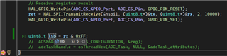
When trying to read a register using SPI, this is what i'm doing:

	uint16_t rx = 0;
	uint16_t tx = (0 << 15) | ((ADS_DEVICE_ID & 0x3F) << 9) | 0x0;
	HAL_StatusTypeDef ret;

	HAL_GPIO_WritePin(ADC_CONVST_GPIO_Port, ADC_CONVST_Pin, GPIO_PIN_SET);
	while (HAL_GPIO_ReadPin(ADC_BUSY_GPIO_Port, ADC_BUSY_Pin) == GPIO_PIN_SET)
	{
	
	}
	HAL_GPIO_WritePin(ADC_CONVST_GPIO_Port, ADC_CONVST_Pin, GPIO_PIN_RESET);
	
	// Send read register command
	HAL_GPIO_WritePin(ADC_CS_GPIO_Port, ADC_CS_Pin, GPIO_PIN_RESET);
	ret = HAL_SPI_TransmitReceive(&hspi1, (uint8_t*)&tx, (uint8_t*)&rx, 2, 10000);
	HAL_GPIO_WritePin(ADC_CS_GPIO_Port, ADC_CS_Pin, GPIO_PIN_SET);

	// Don't care
	ret = HAL_SPI_TransmitReceive(&hspi1, (uint8_t*)&tx, (uint8_t*)&rx, 2, 10000);
	
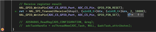
	// Receive register result
	HAL_GPIO_WritePin(ADC_CS_GPIO_Port, ADC_CS_Pin, GPIO_PIN_RESET);
	ret = HAL_SPI_TransmitReceive(&hspi1, (uint8_t*)&tx, (uint8_t*)&rx, 2, 10000);
	HAL_GPIO_WritePin(ADC_CS_GPIO_Port, ADC_CS_Pin, GPIO_PIN_SET);

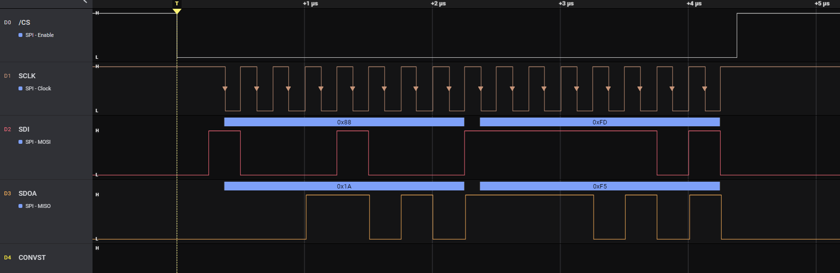
If I comment out the part where I start a conversion by setting CONVST high, the ADC doesn't return anything. Just returns 0x0, as you can see by the image:

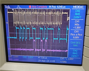
At the final ReceiveTransmit command where i'm supposed to receive the register in it's default state (if I don't comment out the CONVST section), I get readings like this:
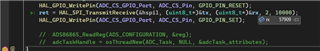
Or this:

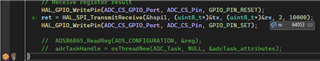
If we take a look at the 8 least significant bits of the value in the rx buffer, I always see the value 0x35 (53 in decimal):

What am I doing wrong? Can someone point me in the right direction here, please? I'm thrilled to use this ADC in my power system protection relay...

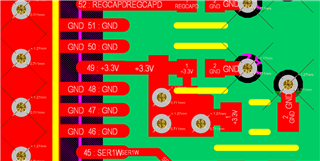
Attached to this post is also the schematics for my design.

protection-relay-schematics.PDF

  • Hi Gabriel,

    Can you provide a screen capture or two of your SPI read and write commands?  The code snippet helps, but a picture is worth a thousand lines of code. 

  • I'm sorry, do you mean a screen capture of a logic analyzer interface when I issue the read commands?

  • I mean something similar to what Dale posted in the original post:

  • I see. I don't have a logic analyzer available atm. In the meanwhile, is there any way you can give me some tips about what might be wrong? Maybe there is something wrong with the schematics? I will be able to get my hands on a Oscope with logic analyzer tomorrow.

  • The only thing in the schematic that gives me pause are the red X's on pins 49 and 51 (sheet 3?) of the ADS8681.  You may be using Altium and that red X sometimes means there is no connection - it could also be a grid error (a warning, not an actual problem), so you might want to verify those connections are actually made.

  • They are indeed connected. That red X does not mean no connection in Altium. It is used to suppress warnings and errors that the compiler might point out. Not sure why I still have those there, but in the layout and the actual PCB they are connected.

  • Cool - will wait for the timings from the LA then.

  • Alright. Please don't close this thread. I committed the unfortunate mistake to not place test points for these signals on this board, so I have some Pomona Electronics test clips on the way tp probe directly at the IC pins. Fortunately it's a LQFP package...

  • Hi, here are the timings.

    I am performing reads to the first seven registers, see the code below:

    	ads8686s_setup(&dev);
    	ads8686s_read(&dev, 0x2, &ret);
    	ads8686s_read(&dev, 0x3, &ret);
    	ads8686s_read(&dev, 0x4, &ret);
    	ads8686s_read(&dev, 0x5, &ret);
    	ads8686s_read(&dev, 0x6, &ret);
    	ads8686s_read(&dev, 0x7, &ret);
    	ads8686s_read(&dev, 0x8, &ret);

    Now it appears it's returning the correct values, but I am still unsure. Can you check the waveforms and let me know?

    I'm using CPOL = 1 (clock is idle high) and CPHA = 0 (sample on first edge)

  • Hi Gabriel,

    This looks good to me!

  • Hi, Tom.

    I'm having another issue now. I'm not being able to increase my SPI frequency above 2 MHz. Up to 2 MHz all the features work fine, but after that the ADC spits out garbage and even fails the self test.

    Signal integrity here is most likely not an issue since the LA captures the data I'm transmitting perfectly. Also, here is a scope view of the signals:

    Please don't mind the overshoot captured by the scope. This is because I'm using a 6 MHz 1x probe and at 4 MHz the edges start to attenuate, so I have set it to 10x, but due to the higher input impedance, I get the ringing that can be seen on the scope. I'm pretty sure this ringing is not coming from the SPI signals since I saw them at the exact same magnitude when feeding the scope with a 4 MHz clock from a very expensive signal generator.

    Also, it's only the data being transmitted by the ADC that looks bad. The data transmitted by the STM32 / received by the ADC looks fine at any frequency.

    Do you have any advice for me in this case? What can I do to be able to get at least 30 or 40 MHz SPI clock? For my application 2 MHz is fine but I'd like to minimize transfer times.

    PS: also probably not PCB layout related, since I have Ethernet RMII to a DP83640 on the same board and the performance is perfect, reaching very close to 100 Mbps.

  • Hi Gabriel,

    I suspect CH3 is your command and that CH2 is SDO from the ADS8686S.  It's a bit hard to tell where the edges line up against the SCLK, but it looks to me like you have some phase shift that might be causing you issues.

    Look at the area that I've circled.  That is a single bit on SDO and SDI and you can see a difference of 1/2 a SCLK cycle between them.

  • Hi, I figured out the issue:

    • After issuing a reset and writing/reading registers to configure the device, It appears that the max clock the device can handle is about 2 MHz;
    • For reading conversion results, the device can work up to the 50 MHz advertised in the datasheet;
    • Also, another issue I've had is that if you try to read the conversion results while keeping the MOSI line high, the next time you try to read the conversion results the ADC will output only zeros. You must keep the MOSI line low (NOP) or send valid commands.

    Now I have the ADC full blasting at 48MHz and it works perfectly. Very impressed with the performance, but the datasheet is not very clear regarding these points.

  • Great news!  Thank you for letting us know.  Will see what can be done to enhance the datasheet descriptions.