This thread has been locked.

If you have a related question, please click the "Ask a related question" button in the top right corner. The newly created question will be automatically linked to this question.

ADC12DL1500: Pin usage and migration guide

Part Number: ADC12DL1500
Other Parts Discussed in Thread: ADC12D1800, LMH6554, LM95241, ADC12DL3200EVM, ADC12DL3200, ADC12DL2500

Tool/software:

Hi,

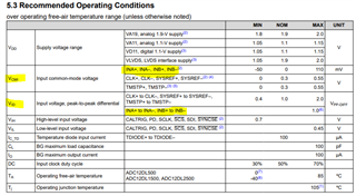
1) I want to migrate my design which is currently using ADC12D1800 to new part ADC12DL1500. Is there any migration guide that's available?

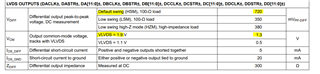
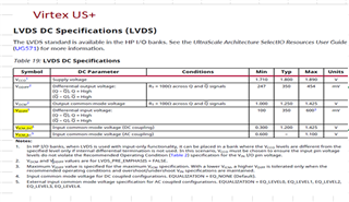
2)  In the old part "V_CMO" pin was available which was used previously used as an input to VCM pin of LMH6554. In the new ADC which is the equivalent pin to that?

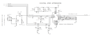
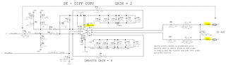
3) Previously we used all data lanes of DI, DID, DQ, DQD to interface with FPGA. With the ports renamed as LVDS A, B, C and D, how do these map to current ADC's DI/DID/DQ/DQD?

4) We plan to retain LM95241 for remote temperature sensing. Is that ok with ADC12DL1500?

Thanks

  • Hello Nandini,

    We do not have a migration guide. But you can look at the ADC12DL3200EVM for a schematic reference (the ADC12DL3200 is a faster speed grade for this family of parts and the pcb schematic is the same for both the ADC12DL1500 and ADC12DL3200)

    This part has no VCMO pin, the common mode of this ADC is 0V and is self biased. For the input VCM to the amplifier you can just ground it.

    For each input there are a maximum of two output LVDS buffers that can be used. Bus A and C are used for input A and B and D are used for input B. Please take a look at the timing diagrams in section 5.11 of the datasheet for a summary of all the different output modes the ADC supports, e.g. dual channel vs single channel demux vs non demux etc.

    If you could give me sometime I will double check on a temp sensor to recommend.

    Thanks,

    Eric

  • Hi Eric,

    Adding on some more queries:

    1. With the current ADC we are running at max frequency 1800/3600. If we change to ADC12DL2500, can we retain the same sampling frequency? 

    2. By default LVDS swing is supposed to be 350mV. But why in this device it is set to 750mV?
    3. Similarly common mode voltage for LVDS is to be 1.2V. But why is it mentioned as 1.9V in the above picture?

    4. I want to interface this ADC to VU23P Ultrascale+ FPGA. I am thinking of connecting VLVDS to 1.1V with LSM mode (350mVpp). Is it ok with below FPGA characteristics?
    5. For the inputs (INA+/-, INB+/-) of the new ADC, we will be connecting them to output of below circuits. 
      What changes are to be done to achieve the Page13 VCMI, VID specifications of new ADC?

    Thanks

  • Hi,

    any response on this?

    Thanks

  • Hi Nandini,

    The DL2500 digital interface is set by default to a double current mode in order to handle and maximize the setup/hold time for data collection. This is particularly helpful when running digital routes across longer trace lengths and back planes.

    You can choose the lower LVDS swing in order to satisfy the FPGA interface requirements.

    The other analog input questions, I see I have answered in another post.

    Regards,

    Rob

  • Thank you Rob.

    Can you pls confirm on this as well from my original post above?

    "We plan to retain LM95241 for remote temperature sensing. Is that ok with ADC12DL1500?"