This thread has been locked.

If you have a related question, please click the "Ask a related question" button in the top right corner. The newly created question will be automatically linked to this question.

ADC12DJ5200RFEVM: Trouble in setting JMODE5

Part Number: ADC12DJ5200RFEVM
Other Parts Discussed in Thread: TSW14J57EVM,

Tool/software:

Hi,

I am trying to check the operation of JMODE5 and am having problems.

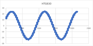
Configuration 1 was able to capture the sine wave input from the function generator to INA.

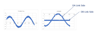
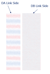
Configuration 2 was able to capture the sine wave for the DA link side data, but not for the DB link side.
When a sine wave was input to INB, the data on the DB link side was able to capture the sine wave, but the DA link side was not able to capture the sine wave.

Have there been any reports of similar problems in the past?

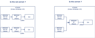
Are the two RX PHYs out of sync? I tried one PHY (8 lanes) as a test, but the data on the DB side is not sinusoidal, so I don't think it is a synchronization problem.

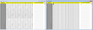
Color map of data acquired by ILA of Xilinx's JESD204 IP output signals.

When in ramp mode or transport layer test mode, both links appear to be storing data correctly.

Test Configuration 1
TSW14J57EVM(RevE) + ADC12DJ5200RFEVM

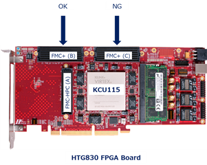
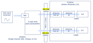
Test Configuration 2
HTG830 (Hitech Global) + ADC12DJ5200RFEVM

Regards,

Takeo

  • Hello Takeo-San,

    JMODE5 of the ADC is a single channel mode, so only one input is active at a time, whenever you switch which input is active between the two analog inputs INA and INB you must run a calibration of the ADC in order for it to take affect. But what you are seeing is strange are you making any other modifications to the ADC at all? From the ADC both links will be aligned, do you have any way of monitoring the link status on the FPGA side? To ensure that all XCVR plls lock, All of the ADC lanes are locking and there are no lane buffer overflows. Finally, can you let me know what FPGA FW you are using to capture data is it TI JESD 204c IP, Xilinx or some other custom solution?

    Best,

    Eric

  • Hello Eric-San,

    Thank you very much for your quick reply. Perhaps there is a mistake in the configuration on my FPGA board.

    HTG830 has two FMC+ connectors, FMC+(B) seems to have a sine wave coming in, while FMC+(C) only has a sine wave coming in on one link.
    FMC+(B) uses one Xilinx JESD204 PHY (8 lanes) since the signals are located in the same SLR (Super Logic Region); FMC+(C) uses two PHYs (4 lanes each) since the signals span SLR0 and SLR1.

    Now, JESD204 parameter K is set to 32 (JMODE5=8bit single channel 8lane).
    So the link parameters for Xilinx JESD204 IP are set as follows.

    Perhaps the blocks are not well placed?

    K Value of ADC EVM Configuration

    Xilinx JESD204 IP Link Parameter Configuration

    Still, it is strange that in ramp mode or transport layer test mode, both links appear to be storing data correctly, but in normal mode, only one link's data is correct. If the two links were out of sync, I would expect the data to be wrong in both the transport layer test and in ramp mode, but that is not the case.

    ーーーーーーーーーーーーーーーーー

    Below are the answers to your questions.

    Q1. But what you are seeing is strange are you making any other modifications to the ADC at all?

    A1. The only change I made to the ADC EVM was to modify it according to the EVM user guide to make it an Onboard Clocking Option. www.ti.com/.../slau640 (7.2.2)

    Q2. From the ADC both links will be aligned, do you have any way of monitoring the link status on the FPGA side?

    A2. I add an ILA and monitor the output signal of the JESD204 IP to verify. (rx_frame_error etc) I am concerned about what should happen to the rx_start_of_frame, etc. for each IP when using two JESD204 PHY IPs and two JESD204 IPs, respectively, as in this case.

    Q3. Finally, can you let me know what FPGA FW you are using to capture data is it TI JESD 204c IP, Xilinx or some other custom solution?

    A3. They are listed below.

    ・Vivado 2020.1

    ・Xilinx JESD204 PHY IP (v4.0)

    ・Xilinx JESD204 IP(7.2)

    ・FPGA Kintex Ultrascale KCU115

    ・FPGA Board => HTG830 (Hitech Global) www.hitechglobal.com/.../Virtex-UltraScale-FPGA.htm

    ※I am not using the TI 204C IP as I am programming with an IP integrator (block design).It would be nice if an IP integrator (block design) compliant version was released.

    Best regards,

    Takeo

  • Hi, Eric-San.

    The problem seemed to be the use of the ADC EVM configuration tool.
    I could not get a sine wave when batch loading registers from the Low Level View tab.

    When I set manually on each tab screen, I was able to get the sine wave.
    If the register settings at that time were saved in a file and this file was used to load a batch of registers, the sine wave could not be obtained.

    I do not know the detailed cause, but I decided to run it with manual settings for the time being.

    Regards,

    Takeo