This thread has been locked.

If you have a related question, please click the "Ask a related question" button in the top right corner. The newly created question will be automatically linked to this question.

ADS131A02: Problem with ADS131A02 and SPI Communication using esp32.

Part Number: ADS131A02

Tool/software:

Hello,

I am using an ADS131A02 and an ESP32-PICO-KIT for my project. In this case, the ADS131A02 is in synchronous slave interface mode, as I will be using SCLK as iCLK. The problem is that I cannot get a response different from "0x7F8100" in the SPI communication.

I have attached the circuit schematic:
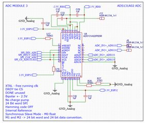

It is also important to consider everything shown in the image, as it contains all the proposed configurations. One of the most important is that the word size is 24 bits, with hamming disabled, SCLK as iCLK, no charge pump. Finally, I do not have a pull-up resistor for the CS pin because I am using the internal pull-up of pin 15 (CS0).

I have also attached the code used:

#include <stdio.h>
#include "esp_log.h"
#include "freertos/FreeRTOS.h"
#include "freertos/task.h"
#include "driver/gpio.h"
#include "driver/spi_master.h"

/* Define GPIO Pins for MOSI and MISO, and SCLK PIN */

#define HSPI_MOSI_GPI 13
#define HSPI_MISO_GPI 12
#define HSPI_SCLK 14
#define HSPI_CS 15

/* Define REG'S for SPI Communications */

//Read Only ID Registers

#define ID_MSB_REG 0x00 //ID Control Register MSB
#define ID_LSB_REG 0x01 //ID Control Register LSB

//Status Registers

#define STAT_1_REG 0x02         //Status 1 Register. (This register is automatically transferred on the command status response when the NULL command is sent.)
#define STAT_P_REG 0x03         //Positive Input Fault Detect Status Register (exceeds the threshold set by the COMP_TH[2:0] bits)
#define STAT_N_REG 0x04         //Negative Input Fault Detect Status Register (exceeds the threshold set by the COMP_TH[2:0] bits)
#define STAT_S_REG 0x05         //SPI Status Register
#define ERROR_CNT_REG 0x06      //Error Count Register. This register counts the Hamming and CRC errors.
#define STATM2_REG 0x07         //Hardware Mode Pin Status Register

//User Configuration Registers

#define A_SYS_CFG_REG 0x0B      //Analog System Configuration Register
#define D_SYS_CFG_REG 0x0C      //Digital System Configuration Register
#define CLK1_REG 0x0D           //Clock Configuration 1 Register
#define CLK2_REG 0x0E           //Clock Configuration 2 Register
#define ADC_ENA_REG 0x0F        //ADC Channel Enable Register
#define ADC1_REG 0x11           //ADC Channel 1 Digital Gain Configuration Register
#define ADC2_REG 0x12           //ADC Channel 2 Digital Gain Configuration Registers


/* Define device to handle*/

spi_device_handle_t spi_device_handle;

/* Function init_spi for configure SPI*/
static esp_err_t init_spi(void)
{
    /* BUS CONFIG FOR INIT */

    spi_bus_config_t  spi_bus_config = {};
    spi_bus_config.mosi_io_num = HSPI_MOSI_GPI;  // GPIO pin for Master Out Slave In (=spi_d) signal
    spi_bus_config.data0_io_num = -1;            // GPIO pin for spi data0 signal in quad/octal mode
    spi_bus_config.miso_io_num =  HSPI_MISO_GPI; // GPIO pin for Master In Slave Out (=spi_q) signal
    spi_bus_config.data1_io_num = -1;            // GPIO pin for spi data1 signal in quad/octal mode
    spi_bus_config.sclk_io_num = HSPI_SCLK;      // GPIO pin for SPI Clock signal
    spi_bus_config.quadwp_io_num = -1;           // GPIO pin for WP (Write Protect) signal
    spi_bus_config.data2_io_num = -1;            // GPIO pin for spi data2 signal in quad/octal mode
    spi_bus_config.quadhd_io_num = -1;           // GPIO pin for HD (Hold) signal
    spi_bus_config.data3_io_num = -1;            // GPIO pin for spi data3 signal in quad/octal mode
    spi_bus_config.data4_io_num = -1;            // GPIO pin for spi data4 signal in octal mode
    spi_bus_config.data5_io_num = -1;            // GPIO pin for spi data5 signal in octal mode
    spi_bus_config.data6_io_num = -1;            // GPIO pin for spi data6 signal in octal mode
    spi_bus_config.data7_io_num = -1;            // GPIO pin for spi data7 signal in octal mode
    spi_bus_config.max_transfer_sz = 4092;          // Maximum transfer size, in bytes

    /*
     DEVICE INTERFACE CONFIG FOR INIT
    */

    spi_device_interface_config_t spi_device_interface_config = {};
    spi_device_interface_config.mode = 1;                     //SPI mode, representing a pair of (CPOL, CPHA) configuration
    spi_device_interface_config.duty_cycle_pos = 128;         //Duty cycle of positive clock
    spi_device_interface_config.clock_speed_hz = 1 * 1000 * 1000;     //SPI clock speed in Hz
    spi_device_interface_config.spics_io_num = HSPI_CS;       //CS GPIO pin for this device
    spi_device_interface_config.queue_size = 1;               //Transaction queue size
    spi_device_interface_config.pre_cb = NULL;                //Callback to be called before a transmission is started
    spi_device_interface_config.post_cb = NULL;               //Callback to be called after a transmission has completed

    spi_bus_initialize(SPI2_HOST, &spi_bus_config, SPI_DMA_CH_AUTO);
    spi_bus_add_device(SPI2_HOST, &spi_device_interface_config, &spi_device_handle);

    return ESP_OK;
}
uint32_t spi_send_command(uint16_t command_adc)
{
    uint32_t command = (uint32_t)command_adc << 8; // 16 bit to 24 bit
    uint8_t data[3] = {0};  // Buffer - 24 bits
    uint8_t zeros[3] = {0}; // Buffer - 24 bits

    // Transacción para enviar el comando
    spi_transaction_t spi_transaction = {
        .tx_buffer = &command,
        .rx_buffer = NULL,
        .length = 24,       
        .rxlength = 0     
    };
    spi_device_transmit(spi_device_handle, &spi_transaction);

   
    spi_transaction_t spi_transaction_resp = {
        .tx_buffer = zeros, 
        .rx_buffer = data,
        .length = 24,   
        .rxlength = 24  
    };
    spi_device_transmit(spi_device_handle, &spi_transaction_resp);

    //
    uint32_t response = ((uint32_t)data[0] << 16) | ((uint32_t)data[1] << 8) | (uint32_t)data[2];

    //uint32_t response = data;
    
    return response;
}
static esp_err_t ads131a02_init(void)
{
    gpio_pullup_en(GPIO_NUM_15);
    uint32_t valor = spi_read_register(0x03);
    char str[32]; 
    snprintf(str, sizeof(str), "%lu", (unsigned long)valor);
    printf("Response: %s\n", str);

    return ESP_OK;
}

void app_main(void)
{
    ESP_ERROR_CHECK(init_spi());
    ESP_ERROR_CHECK(ads131a02_init());
}


I know the error could be in the programming or the schematic because when I measure the REFP value, it gives me 1.25 V by default but negative, relative to GND. The capacitors are non-polarized ceramic capacitors. I appreciate your help as I have tried to solve this and haven't been able to.

  • Hi Juan Esteban Botero Rodriguez,

    The ADC appears to be setup correctly, given the information you have provided

    Can you provide logic analyzer plots showing the data you are sending to and receiving from the ADC?

    You might also try operating in asynchronous interrupt mode to make sure you get can valid data out of the ADC, this is usually the easiest mode to get working

    -Bryan

  • Hi, Bryan.

    I'm currently conducting tests with the logic analyzer; once I have all the evidence, I'll attach it. I'll test the asynchronous mode as a last resort, as it would require changes to the designed board. Thank you very much for your response, and I'll send a reply as soon as I can.