This thread has been locked.

If you have a related question, please click the "Ask a related question" button in the top right corner. The newly created question will be automatically linked to this question.

ADS131E08: Read Data with RDATA command and the result is corruption

Part Number: ADS131E08

Tool/software:

Hi,TI's specialist.

When I used ADS131E08 to collect data, the data I returned was wrong, and I used RDATA  command . The hardware interface is that the power supply AVDD = 3.3V, the internal clock of the chip is 2.048MHZ, and the single-ended signal is input with (CH1~CH6).

The MCU used is C2000 DSP280039, and my software configuration process is as follows:

1. Initialize SPI, 4MHz, 16bit, Polarity 0, phase 0;

2. RESET ADS131e08 according to manual 11.1 Power-Up Timing;

3. Send SDATAC command and send STOP command;

4.  Confg1 0xd2h, Multiple data readback mode,  sampling rate of 16KSPS;

5、Confg3 0x40h, using external reference source (3V);

6、channel registers to configure 0x10h, with CH1~CH6 enabled and CH7 and CH8 disabled;

7、Send a START command;

8、 Change the SCLK frequency of SPI to 10Mhz;

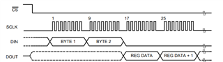
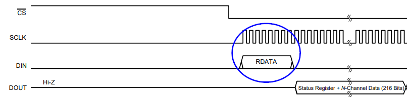
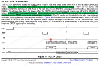
Next,I sent a  RDATA command in the 15KHz EPWM interrupt function, and sent the remaining 216 SCLks to read the data of eight channels. The CS pin was kept low throughout the process. Because the interrupt frequency of 15K is asynchronous with the set sampling frequency of ADS131E08, there will be a phenomenon that the DRDY event overlaps with the reading data clock SCLK, but the manual says that it will not cause data corruption, which can be seen in the actual test.

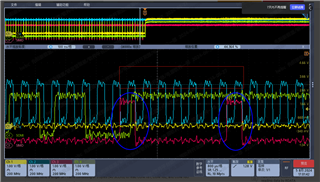
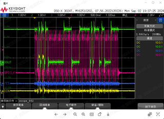
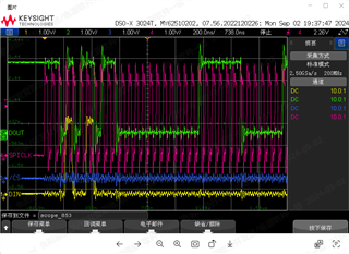
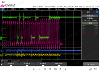
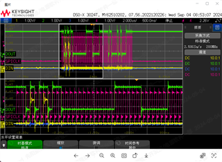
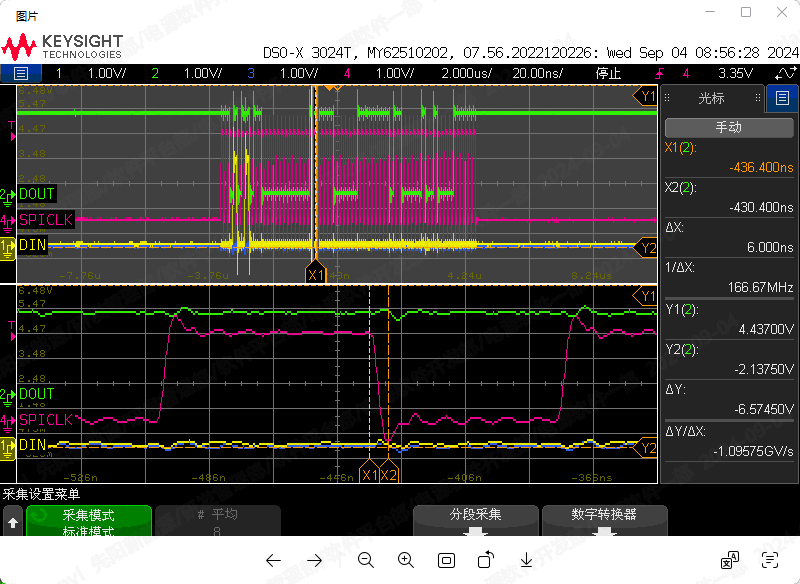
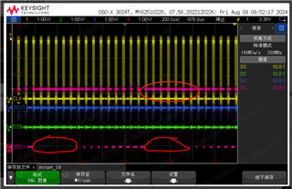
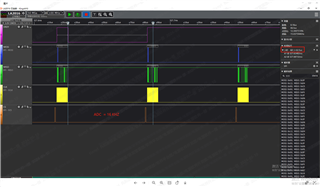
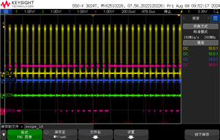
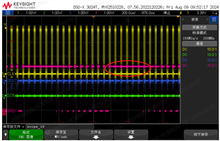
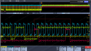
Oscilloscope waveform:

1-> SCLK; 2->DOUT (MISO); 3->DIN (MOSI) ;4->DRDY

Data corruption occurs at the following moments:

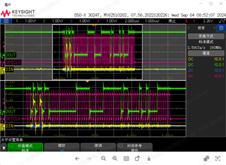
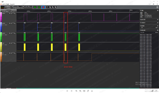
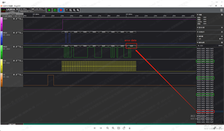
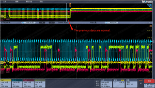
We did a test on related data errors time, and the test method is:

1、 Only the upper 8 bits of channel 2 data (the upper 8 bits of 24-bit data) are read, because the input of channel 2 is about 1.5V If the data changes suddenly, the upper 8-bit data will change. The difference between it and the above configuration is: SPI Polarity 1, phase 0.

2、If the high 8bit data will change, pull up the CS pin and grab the oscilloscope waveform through it.

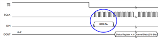
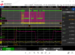
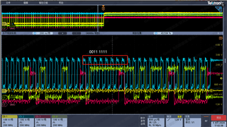
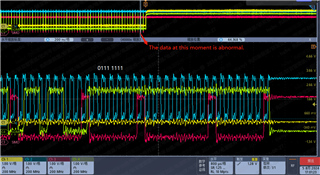
Waveform at normal time of data: 1: CS; 2、SCLK; 3、DIN (SIMO) ; 4、DOUT(SOMI)

Normal data high 8 bits 0011111 :

High 8 bits of data at abnormal time 011111 :

Finally , Does the DRDY event really affect data reading when using the single conversion instruction RDATA? 

We want to know what the problem is. Looking forward to your reply, thank you!

  • Hello,

    It appears that you are using different SPI modes.  The ADS131E08 should ALWAYS use SPI settings CPOL=0, CPHA=1.  SCLK should idle low, the ADS131E08 captures data (DIN) on the falling edge of SCLK and launches data (DOUT) on the rising edge.  The host processor should also launch data on SCLK rising edge (MOSI), and should capture data on SCLK falling edge (MISO).

    You are writing to CONFIG1 and CONFIG3 registers.  As a test, I suggest reading the values back from these registers to confirm that you have everything configured correctly.

    You could send a single SPI frame consisting of 5 bytes (40 SCLKs) to read CONFIG1, CONFIG2, and CONFIG3.

    Send 0x21 02 00 00 00h and confirm the values of the CONFIGx registers.

    Also, use the scope and monitor the DRDY line; this should be toggling at the expected data rate of 16kHz.  Please also provide a picture of the schematic showing all pin connections to the ADS131E08.

    Using the RDATA will always readback valid results.  However, if you are not reading data fast enough, then you will simply miss conversion readings, but the readings you get will be valid.  From what I can tell, it looks like you may still be in the power-up default RDATAC mode.

    Regards,
    Keith Nicholas
    Precision ADC Applications

  • Hello,Keith Nicholas

    The schematic design used is as follows:

    At the beginning, the SPI mode used was also SPOL=0 and SPHA=1, but communication could not be established normally. However, using SPOL=0, SPHA=0 or SPOL=1, SPHA=0, communication can be established normally.

    At the same time, we attempted to use an emulator to read the register configuration, which was consistent with the required settings.

    At the beginning of initialization, we try to send the SDataC instruction. After initialization is complete and register configuration is completed, we try to send the SDataC instruction again before reinitializing the SPI rate and reading the converted data. All subsequent data reading processes send RData instructions.

    Looking forward to your reply, thank you!

  • Hello,

    The schematic looks O.K., you should be able to read conversion results from the ADC.  However, it is very important that the bypass capacitors are placed very close to the supply pins on the part.  For best performance, we recommend individual bypass capacitors for each power supply pin on the ADC.  I these capacitors are not close to the ADS131E08 package, you could have unpredictable operation.

    Please capture the first part of the SPI frame that captures data.  Just capture the first 56b (SCLKs), which include the RDATA command, STATUS word, and the channel1 conversion result.  Include 1: CS; 2、SCLK; 3、DIN (SIMO) ; 4、DOUT(SOMI) as before.  I would like to verify that the timing is correct.  Also, when you capture this data, please provide a constant input voltage and let me know the value of the voltage to see if the conversion results are correct.

    Also, looking at your previous waveform capture, the DIN (SIMO) has activity on it, circled in BLUE below; the DIN should be low during channel data readback.  The only time there should be activity is during the first 8 SCLKs of the SPI frame when sending the RDATA command.

    Regards,
    Keith

  • Hello,Keith Nicholas

    The SPI configuration is set to 16 bit mode, and the ADC configuration is set to 16KHZ,Polarity 0, phase 0. The following figure shows the 64 bit data of the SPI frame, including the RDATA command, STAT3 word, and the conversion result of channel1. The data for channel 1 is 1.5V, and the external benchmark is 3V.


    In addition, during the data retrieval period, DIN is not at a low level because the amount of data is too large. In order to facilitate data reading, DIN is assigned a special value and avoids command words. The measured data does not seem to be affected by this factor.

    Looking forward to your reply, thank you!

  • Hello Zhang,

    It appears from your scope plots above that you are using f-SCLK=20MHz.  (4 SCLK periods in 200ns).  Since it is hard to tell if setup and hold times are being met, I suggest reducing F-SCLK to a much lower frequency, such as 8MHz, to rule out any timing issues.

    Also, when reading data from the ADS131E08 using RDATA command, I suggest you keep DIN low after sending RDATA (12h) for the rest of the frame.  Even though you are not sending a valid command, the ADC still must process the data, and if it is an unexpected value, you may get unexpected behavior.

    Regards,
    Keith

  • Hello,Keith Nicholas,

    The following figure shows that the SPI rate is 8MHz, and everything else remains the same as above. In fact, we have tried reading data at a lower rate and obtained the same result.

    In practical use, after sending the RDATA command, we lower the DIN, but the result is still the same.

    Looking forward to your reply, thank you!

  • Hello Zhang,

    Keeping DIN low after the RDATA command is sent, are you now able to read the correct conversion results?  Have you sent a full RDATA frame, consisting of RDATA (8b), STATUS (24b) and 8 channels of conversion results (8x 24b)?

    Set /CS low

    Send RDATA, 8x SCLK

    Send 24x SCLK, capture STATUS

    Send 192x SCLK, capture 8x Channels

    Set /CS high, end of SPI frame, resets SPI port

    Regards,
    Keith

  • Hello,Keith Nicholas,

    After sending the RDATA instruction, keeping DIN at a low level still has the same issue as the initial one, which is reading data abnormally when the ADC completes the conversion of new data. What we are sending is a complete data frame, consisting of 224 * SCLK, including RDATA (8b), STAT3 (4b), and conversion data from other channels (8 * 24b).
    In addition, we only used one SPI peripheral, so/CS is a fixed low level, which should not affect the normal reading of data?

    Looking forward to your reply, thank you!

  • Hello Zhang,

    Although you can keep /CS pin low for multiple conversion cycle readings, I do not recommend using this approach.  Any glitch on the SCLK will be interpreted by the ADC as an additional clock, and will corrupt communications.  Once communications are corrupted, you will need to reset the SPI port by taking /CS high and then back low again.  I recommend you use /CS for each conversion cycle reading to reset the SPI and minimize the effects of noise on the SCLK line.

    I had assumed you were actively using /CS for each frame; since you are not, this does explain why you are getting bad readings after a period of time.  You can reduce the noise on SCLK by properly terminating with a series resistor near the SCLK source on your processor, as well as good ground layout on your PCB.  However, any transient in the system, even with a very good layout, can still cause problems over a long period of time.  For this reason, and to improve your communications, you should use the /CS for ADC conversion readings as I outlined before.

    Regards,
    Keith

  • According to your statement, we set the CS signal to a high level before each data read to reset SPI, and then pull down the chip selection to re read the data. However, the results we obtained were consistent with the initial ones and did not show any improvement.
    In fact, not all channel data is read abnormally, it is only when the SCLK read from a certain channel data happens to have an exception when the ADC new data conversion is completed.

    Looking forward to your reply, thank you!

  • Hi Zhang,

    I need to discuss with my team and will get back to you by end of business on Monday.

    Regards,
    Keith

  • Hi zhang qiu,

    In the image below that you sent previously, you can see that DRDY stops toggling during the time you said you were receiving "data corruption". If DRDY stops toggling, this means the ADC is no longer converting, or at least that the ADC has restarted the conversion process.

    It is not clear to me what is causing this issue, so can you try the following:

    1. Use CS to frame the RDATA command (note that SCLK >4MHz to clock out all of the data). This means that every time you send a command, CS should start high, then you bring CS low, send the command, then bring CS back high again to end the frame
    2. Keep DIN low the entire frame other than the RDATA command
    3. Use the DRDY signal to trigger the data readback when there is a high-to-low transition instead of using an asynchronous timer. This means you need to write FW to look for the DRDY transition, then send the RDATA command, then clock out all of the data (framed by CS of course)

    This is how we would expect the ADC to be operated, so this should work very well.

    Please send us a scope shot showing what happens when you do this. Also, you might need to provide us logic analyzer plots instead of oscilloscope so we can see the whole data transaction. It is very difficult to diagnose the issues you are having using these scope shots

    Also, you mention that the signals you are measuring are single-ended:

    The hardware interface is that the power supply AVDD = 3.3V, the internal clock of the chip is 2.048MHZ, and the single-ended signal is input with (CH1~CH6).

    Note that the ADS131E08 cannot measure single-ended (ground-referenced) inputs when using a unipolar supply (AVDD = 3.3V in your case). This is evident by equation 4 in the datasheet, which I have copied below

    -Bryan

  • Hello  Bryan,

    We use the first and second points you mentioned, and there will be exceptions when reading data. But based on the third point you mentioned, we have adopted a DRDY peripheral interrupt method to read data, and the data is normal, which can avoid the occurrence of data anomalies.
    However, according to the manual instructions, using RDATA command should not require checking DRDY, that is, it can read data asynchronously. However, the actual phenomenon conflicts with the manual. Therefore, should we use RDATA to determine whether it can perform asynchronous operations (here, asynchronous operations do not require checking whether DRDY has changed, that is, normal data can be read at any time).
    Our question is: Is it an error in the manual instructions or is it due to our incorrect use of the RDATA command.
    In addition, the relevant instructions in the manual are attached below:

    We used a logic analyzer to capture abnormal data waveforms, where the timing met your requirements for the first and second points, but the third point was not met (because we wanted to verify whether our question was correct). Among them, only 64 SLCKs were read, and the last byte (0x3F) is the highest bit data of channel 1, where 0x3F is the correct data.
    At the same time, we captured the highest bit data of channel 1 at the time of DRDY signal overlap. According to the analysis of the logic analyzer, the data (0x5F) is abnormal, which indirectly confirms our hypothesis (DRDY overlap does affect the correctness of the data, and the manual indicates an error).
    We just need you to confirm whether our hypothesis is correct.
    The image of the logic analyzer is as follows:

    Looking forward to your reply, thank you!

  • Hi zhang qiu,

    It seems like there is an issue with the command being sent just before, during, or immediately after (a few microseconds) of DRDY toggling high to low. So this is not an issue with the data per se, but the command. This is effectively stated in the datasheet, but it could be worded more clearly.

    Since you are sampling asynchronously, eventually this condition will occur and you will get bad data. This e2e posts hints at this issue: https://e2e.ti.com/support/data-converters-group/data-converters/f/data-converters-forum/615552/ads131e06-corrupted-data-with-rdata-command

    My recommendations for your system:

    1. Keep DIN low the entire time you are clocking out data. I know you said there were no issues so far, but there definitely could be in the future. You do this at your own risk
    2. Toggle CS before and after data read back. Tying CS low is possible, but not recommended because there is no way to reset the SPI interface without toggling the RESET pin (or powering up/down the ADC). However, it should work
    3. Use DRDY as an interrupt to determine when to read data i.e. read data synchronously to DRDY. This will avoid the RDATA command shifting in time, and eventually "colliding" with the DRDY toggling high to low, which causes data corruption

    -Bryan

  • Hi Bryan Lizon,

    We will adopt your suggestion, thank you very much.

  • Hi he bc,

    Understood, thanks for confirming. If you need anything else, please start a new thread and we will support you there

    -Bryan