ADS127L21: ADS127L21 exhibits a long settling time when using MUX

Part Number: ADS127L21
Other Parts Discussed in Thread: TMUX7209, OPA827, OPA828

Tool/software:

Hi Team

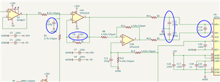
I am encountering a problem while multiplexing ADS127L21 using analog switches, as shown in the schematic below.

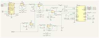
VIN_1, VIN_2, and VIN_3 are all DC signals, R3 and R4 form a voltage divider in order to extend the input range up to 20V. U3A provides an offset of about 30mV to prevent ADC saturation. The two OPAs of U4 are used to convert input signal from single-end into differential, and the common voltage is obtained by R10 and R13 from REF voltage division.

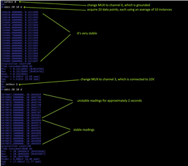
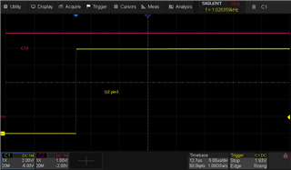
The problem is that when the MUX switches between two voltages with large differences, it takes a long time for the measurement value to stabilize at a few LSBs.

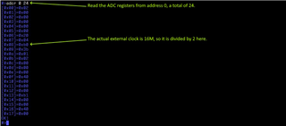
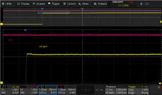
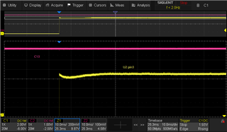
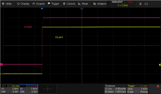
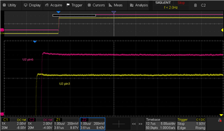
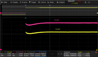
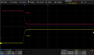
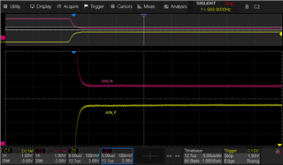
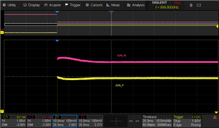
For example, set VIN_1 = 10V, then switch the MUX from S1 to S2 and delay a dozen milliseconds which I think is enough. Then the ADC makes continuous measurements. It can be observed that the first measurement value has an error of approximately dozens of uVs, and then the error gradually decreases, and stabilizes to a constant value after about 1 second.

The stabilization time depends on the voltage difference when switching, the greater the voltage difference, the longer the time takes. According to my tests, the relationship between them is not linear, so it cannot be calibrated out.

This problem has been bothering me for many days, and I can't find any theoretical support for this phenomenon by analyzing the circuit. Can you give me some inspiration from experience?

Best regards.

  • Hello Zhenrong,

    This is likely due to dielectric adsorption (DA) in some of your filter capacitors, specifically C6.  All capacitors that can see time-varying signals should be ceramic NP0/C0G dielectric to reduce the effects of DA.  Since C6 is 100nF, I am guessing you are using a standard X7R or similar ceramic capacitor, which would explain extremely long settling times.

    You can get 100nF capacitors in NP0/C0G dielectric; I suggest ordering some of these and replacing C6.  As a quick test, simply remove C6 and then retake settling measurements to see if this is the primary cause of the slow response.

    In addition, the ADS127L21 internal digital filters will also have a settling time.  You would only see settling times approaching 1s if you are using very high OSR settings resulting in very low data rates.  The settling time for the internal filter is documented in the datasheet; I suggest using one of the low-latency filters and depending on your data rate, you can see the total latency (or settling time) as specified in Tables 7-9 and 7-12 of the ADS127L21 datasheet.

    Regards,
    Keith Nicholas
    Precision ADC Applications

  • Hi, Keith 

    I need to apologize for this; the annotation for C6 in the schematic was incorrectly labeled, it is actually 220pF. The mistake happened when its symbol was copied from C12. It's my badStuck out tongue

    C5, C6, C11, C14, C15 and C19 are all of the C0G type capacitors. And in my design, I have configured the ADS127L21 with the following parameters:

    8MHz external clock, mid-speed mode, sinc3 filter, OSR=80000, REF&AIN buffers on, start/stop control mode,  idle mode.

    So, the data rate is 50sps, and the delay of the sinc3 filter should be 40mS. Moreover, the delay of the sinc3 filter will not be reflected in the output data, the first data is already the delayed data.

    Best regards

  • Hello Zhenrong,

    O.K.  The digital filter will settle in less than 40mS, assuming that you are using the START command after changing the MUX channel setting.

    Based on your schematic, you are using a 5V reference voltage.  In this case, you cannot use the REFP buffer, since it requires 0.7V of headroom from  the AVDD1 supply.  Also, with the AIN buffers, you will be limited to 0.1V to 4.9V when AVDD1=5V.  I am not certain if this is causing the settling issue, but it does need to be corrected.

    I would start looking at the input chain.  Use an oscilloscope and measure the REF output on C13, as well as the outputs of U4a and U4b, looking for any kind of gross errors, such as over/under shoots, as well as oscillations.

    Also, since both the input amplifier and the reference buffer are powered from +25V/-5V supplies, you need to ensure the outputs do not exceed the ABS ratings of the ADS127L21.  With a single 5V supply, this limit will be -0.3V to +5.3V.  I would suggest adding Schottky clamp diodes on the outputs of these amplifiers to protect the ADC inputs in case of a floating input, or some other transients.

    Regards,
    Keith 

  • Hi Keith,

    I have disabled the REFP buffer and the AIN buffer, but the problem persists.

    This is the ADC register configuration.

    This is the result of data acquisition, and no delay was added between the MUX switch command and the data acquisition command. The data rate is 50Hz, but each displayed data point is the average of 10 data points, resulting in an interval of 200mS between each output data.

    Then, I measured the signal input chain with oscilloscope.

    This is the voltage change on pin3 of U2 and C13 when the MUX changes, along with their magnified views at different time bases.

  • This is the voltage change on pin3 and pin6 of U2 when the MUX changes, along with their magnified views at different time bases.

  • This is the voltage change on AIN_P and AIN_N of U5 when the MUX changes, along with their magnified views at different time bases.

    The signal input chain seems to be fine.

  • Hello Zhenrong,

    The scope plot shows that there is no obvious oscillation issues, which can sometimes show up as small offsets when averaged by an ADC such as the ADS127L21.  However, the oscilloscope does not have enough resolution to observe 10's of uV changes.  For this, you would need a good benchtop DMM with very low noise measurements out to single uV levels.

    The settling time is to within 2ppm, and then takes several seconds to settle to within the noise level of your mesaurements.  This is most likely something in the input signal chain. 

    You are measuring 10V; is this the reference voltage?  The input multiplexor can cause a charge kickback due to capacitance on the MUX output.  This may be causing the reference to have a long settling time to recover to less than 1ppm levels.

    Also, what are the physical size of the resistors you are using to scale the 10V input?  If these are 0402 or smaller, you may be getting thermal drift changes that could explain the long settling time.  In this case, you would need to either use larger resistor packages, or a lower thermal drift resistor to reduce the long settling times.

    Regards,
    Keith

  • Hi Keith

    As shown in the figure, the measured 10V voltage comes from the amplified output of a DAC, namely DAC_VOUT. The resistors used for voltage scaling are all of size 0805, with a temperature coefficient of 10ppm, whether input chain or output chain. 

    C26 is a C0G capacitor, and C25 is a metallized polyester film capacitor from KEMET. I have tried replacing C25 with a tantalum capacitor, or shunting a 10nF C0G capacitor with, but there was no improvement. 

    I have also tried using two lithium cells in series (about 8V) as the input signal, and the same phenomenon occurs.

    The charge injection of TMUX7209 is only 3pC, which I believe should be sufficiently low for my design. However, I noticed that it has a capacitance of over 100pF, is this the key of the issue?

    Best regards

  • Hello Zhenrong,

    The 100pF may be part of the problem.  Since this is a DAC output, instead of changing channels, just keep the input channel on the DAC input and then change the DAC value from 0V to 10V; this will eliminate any multiplexor concerns.  The total settling time should be less than 1ms, assuming the dielectric adsorption of the 1uF C25 does not cause a long settling time to a final value.  If it does, you could remove the 1uF cap and check again.

    Regards,
    Keith

  • Hi Keith

    I have done some tests in the last few days.

    First, I followed your instructions and used the DAC to generate a step signal from 0 to 10V without MUX changing. The amplitude of the instability has decreased to approximately 3uV, but the duration of the instability remains unchanged.

    Then I used the DAC to generate a step signal from 0 to 20V, and the amplitude of the instability increased sharply.

    Finally, I used the DAC to generate a step signal from 0 to 5V, and the instability disappeared. By fixing the DAC output at 5V and then generating the same step by MUX changing, no instability occurred either.

    It is clear that when the SR of the step signal is too high, problems occur. However, with low SR such as a step from 0 to 5V, or a step from 0 to 10V generated by the DAC(its SR is much lower than that produced by MUX changing), there are almost no issues. At the same time, I replaced U4 with an OPA that has a larger SR, but there was no change. Therefore, I think the problem may lie with U2. The OPA827 might require more recovery time when the SR of the input signal is too large.

    My question is, is the OPA827 a MUX-friendly OPA? In my understanding, JFET OPA is inherently MUX-friendly. Any way, I will replace U2 with a MUX-friendly OPA such as OPA828 for further testing later.

    On the other hand, there are no issues with a falling step, such as from 10V to 0V or even from 20V to 0V. It's very confused.

    Best regards

  • Hello Zhenrong,

    You may want to post a separate e2e thread specifically for the OPA827 or OPA828.  The product team that supports these devices will be able to provide more insight into any 2nd and 3rd order settling time effects that these devices may have.

    Yes, in general, JFET devices are MUX friendly, but there are different levels of performance.  The OPA828 does high-lite the MUX friendly feature, so this may be the better amplifier and may help improve your results.

    Regards,
    Keith