This thread has been locked.

If you have a related question, please click the "Ask a related question" button in the top right corner. The newly created question will be automatically linked to this question.

ADS131M04: ADS131M04 Not able to communicate with the IC

Part Number: ADS131M04
Other Parts Discussed in Thread: TMS320F28379D,

Tool/software:
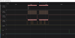
(gui output)

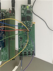
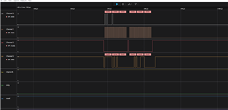
ads131 GUI gives the correct result when I want to read the id register, but when I want to read the id register myself, I cannot communicate with ic, it gives only 0xFF as an answer, my cpol cphase settings are correct, and I also reached the same result when I tried by toggling the reset pin, what could be the reason why I cannot communicate with the device, I use tms320f28379d as a processor, and when I proceeded with the steps in the sample code, I could not get a response from the device.

(code output)

  • Hi Aleyna,

    it almost feels like as if the device is not powered up or is held in reset. Otherwise the device would usually not output all zeros.

    Could you check if the DRDYn pin transitions high after power up? That is an indication that the device is ready for communication.
    Also, did you make sure to provide an external clock at the CLKIN pin?

    Regards,
    Joachim Wuerker

  • (code output)

    (GUI output)

    i checked what you said, I see a value when I read the ID register now, but this value is different from the value read from the GUI, what could be the reason for this? 

    Thanks,

  • Hi Aleyna,

    it looks to me as if your data on DIN is changing on the falling edge of SCLK. However the ADS131M04 latches data on DIN on the falling SCLK edge. Means your SPI CPHA seems to be configured incorrectly.

    Regards,
    Joachim Wuerker

  • My SPI settings are as in the image It seems to be suitable for ads101in datasheet 

  • Hi Aleyna,

    I am not an expert on the TMS320F28379d and what those settings are. I can just comment on what I see in your scope plots.
    I also want to note that CPHA=1 is not always consistently defined the same way by everyone. In the end you need to make sure that the MCU changes the signal on MOSI only on SCLK rising edges.

    Regards,
    Joachim Wuerker

  • First of all, thank you for your answers, device JP1de 5-6 I connect the power to the top and the ground to the bottom of the installed channels, the device does not respond to the ID read command below 2.5V, that is, it does not work Above 2.5V, I obtain the device ID correctly, but the adc data comes 0x7FFFFF, what is the reason for this? Also PGA gain register value 1 for channel0

    (2.6V ID register read correct)

    (2.6V channel0 data 0x7FFFF)

    (2V ID register not responding)

    (2V channel data0x0000)

  • Hi Aleyna,

    I don't think I can follow what exactly you are doing.
    If you reduce the supply voltage below 2.7V, the device will not work anymore at certain point. At that point you will read all zeros.

    Reading 0x7FFFFF indicates that you are reading a positive full scale signal (+FS). If you are using gain=1, that means your differential input signal is >VREF=1.2V. If you connect the supply to the positive analog input and GND the negative input, then this is expected.

    Table 8-10 in the datasheet shows the data format of the ADS131M04.

    Regards,
    Joachim Wuerker

  • Hi Joachim,

    I think I can not fully explain the supply voltage is already provided by the PHI evm controller, when my input signal is below 2.5, I read 0x0000 in the ID register, so I read the ADC channel data 0x0000, when it is above 2. 5, I read the ID register exactly, but I read the ADC channel0 value 0x7FFFFF, I wonder if you have any idea what is the reason for this.

    Thanks,

  • Hi Aleyna,

    could it be that you are collapsing the supply to the ADC in some way with your connections? You might want to measure the supply voltage at the ADC pins to double check.
    As I said, I cannot completely follow how you are applying the input signal to the device. If you could explain that in more detail, that would be helpful.

    Regards,
    Joachim Wuerker

  • Hİ Joachim,

    We solved the problem, I don't know why, but when I receive power from the computer with PHI, the data I read when the JP9 pin receives LDO 3.3v shows 0x7FFFF, but when I feed the power myself, I can read the values properly when I plug the JP9 pin into MSP3v3 and give power from AVDD. I don't know why it doesn't work with USB PHI from the computer, but our problem was solved by running it the other way.Do you have any idea why it does not work with PHI connected?

    Thanks,

  • Hi Aleyna,

    thanks a lot for the positive update. That sounds good.

    I still struggle to understand all your connections to be honest. Previously you also mentioned some connections on JP1. I would probably need a drawing or mark-up in the schematic to understand all your connections and jumper settings.

    If you are reading 0x7FFFFF, that means your differential input signal you are applying is >1.2V.
    When you are reading 0x000000, then the supply of the ADC probably collapsed because you are drawing too much current somewhere. USB can only provide a limited amount of current.

    You could for example measure the input signal and the ADC supply pins with a DMM to see where the problem is.

    Regards,
    Joachim Wuerker