This thread has been locked.

If you have a related question, please click the "Ask a related question" button in the top right corner. The newly created question will be automatically linked to this question.

ADS127L11: Typical Characteristics

Part Number: ADS127L11

Tool/software:

I want to know how the 6.11 figure in datasheet was tested.

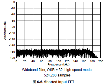
What’s the meaning of "Short input FFT"

What is the output(y axis) in the graph ?

 From which terminal(pin) this amount is measured ?

What does this data represent about ADC performance? It doesn't seem like data like ENOB is intuitive and generic ?

I would like to have an answer from the relevant engineer . THANKS!

  • Hello Junjia,

    This data was taken with the ADC inputs shorted together, and connected to a mid-supply (2.5V) common mode voltage.  Pins 1 and 2 of the RUK package shorted and connected to 2.5V with respect to AVSS.  AVDD1=AVDD2=5V, AVSS=GND and Vref=4.096V.

    The y-axis is dB relative to full scale input, or dBFS.  With Vref=4.096V, the maximum rms voltage of a sinewave will be 4.096/sqrt(2)=2.896Vrms.  Each of the frequency bin peaks are -170dB or lower.  The maximum rms voltage of each frequency bin will be 2.896V*10^(-170/20)=9.159nVrms.

    The primary purpose of providing this data is to show that there are no significant noise spurs (or tones) in the spectrum; the noise is primarily flat and due to thermal noise.  

    ENOB requires a sinusoidal input signal near full scale; you could estimate dynamic range or effective resolution, but you would need the detailed data for the plot.  For these measurements, it is better to use a histogram and directly calculate the total noise.

    Regards,
    Keith Nicholas
    Precision ADC Applications

  • Thank you for your answer.

    from your answer:"The maximum rms voltage of each frequency bin will be 2.896V*10^(-170/20)=9.159nVrms." 

    Are these equivalent input noises also measured at the input? Or is the relevant conversion done via the output digital code values?