This thread has been locked.

If you have a related question, please click the "Ask a related question" button in the top right corner. The newly created question will be automatically linked to this question.

ADS131B04-Q1: SPI Timing

Part Number: ADS131B04-Q1

Tool/software:

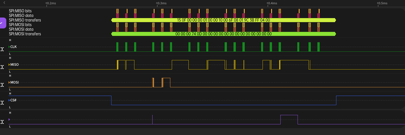
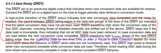
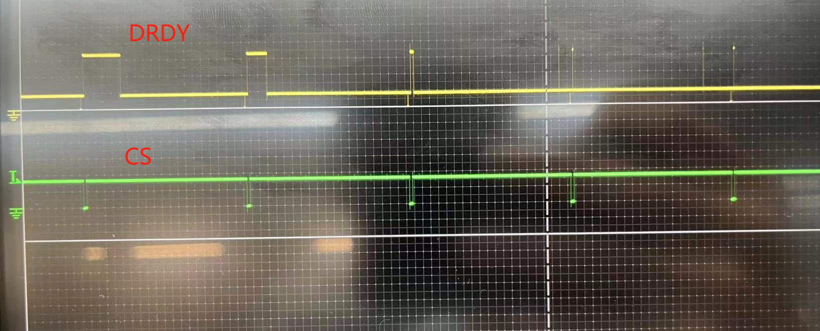
When the MCU communicates with the ADS131B04 SPI, it is observed through the oscilloscope that the DRDY signal is mostly kept low in the SPI timing, and there will be a jump when there is data transmission, is this correct? Because I see that the DRDY written on the data sheet seems to be always high, providing a falling edge when there is data ready

  • Hi ? ?,

    The DRDY pin behavior is explained in the datasheet, see section 8.5.1.5. I copied a relevant portion below

    The DRDY pin stays low when data are not clocked out, or if you start clocking out data but do not clock out the whole frame. Then, the DRDY pin quickly toggles high then back low again to indicate new data are ready. I would guess that this is what you are seeing

    -Bryan

  • I see this section about DRDY in the datasheet and I port the code that TI provide. But DRDY is always low until the data is ready. Do you know why is this happened and what I should do.

  • Sorry, I also want to know that is there any change that needs to be made to the readData operation in the global chop mode in addition to configuring the corresponding registers?

  • Hi ? ?,

    Can you send a logic analyzer plot showing the communication signals from/to the ADC? And please identify on those images what you are seeing with the DRDY pin that is not what you expect. It is hard to tell what is going on from the description you provided

    It seems like you tried to include an image in your post but it did not come through.

    -Bryan

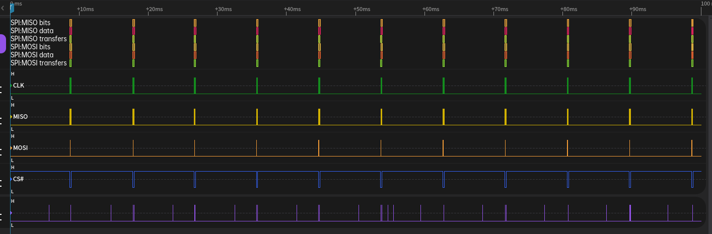
  •  Can you see this?GC_DLY[3:0] is set  1110b(32768/(4.096*10^6)), but the sample period is set 10ms

  • 1、(CLKIN is set 8KHz)The abnormal DRDY behavior still fetches the correct data, and the in-program read data behavior is triggered by an external interrupt on the DRDY pin. When I run the command to read the data every 10ms in the loop, the oscilloscope shows an anomaly as shown in the figure above, and only when the cycle period is set to about 8ms can I get normal DRDY behavior, and the DRDY period is about 9ms. I wonder why

    2、And when I disable input CRC, why sendcommand() and writesingleresgister() behave normally, but I can't get the data, and the 0x2020 always appears.

    3、When running the global chopper mode, do you only need to read the data as usual, because I read the similar behavior of averaging the data several times written in the manual, there is a t(GC_CONVERSION) cycle time, can you tell me more about the operation of running the global chopper mode

  • Hi ? ?

    I did not get a chance to look at this today, but I will respond back tomorrow (Wednesday)

    Thanks for your patience

    -Bryan

  • HI ? ?,

    Do you have a logic analyzer instead of a scope? I would like to see all of the digital signals at one time (SCLK, CS, DRDY, DOUT, DIN). I also cannot see the time scale on your image, so I cannot really tell what is going on

    The image you show looks like you are taking a long time to clock out all of the data. That is why the DRDY stays low for most of the frame. This again is why the logic analyzer would help, so I can see all of the communication to and from the ADC

    Please provide the logic analyzer data so we can help you further

    -Bryan

  • Fig.1Fig.2

    Fig.4Fig.3

    The first is a communication sequence of information, DRDY is a purple line, in the figure you can see that the DRDY always stays low, after a data read out will become high, but the time is very short, then ushered in a falling edge. A wider range of information can be seen in Figure 2. Figure 3 is the information read by the MCU, corresponding to the timing of Figure 4, but perhaps because of the accuracy of the logic analyzer, the logic analyzer shows some errors. Although DRDY showed strange behavior as shown in the picture, the data read was still correct. Could you help me explain this phenomenon? In addition, the time I cycle to read data is 10ms, 32768 when I set GC_DLY, the external clock selects 8MHz, this time the interval between the two frames is about 8ms, so the SPI timing is read like this, only when the cycle read data time is set to 8ms, the SPI timing is correct. But since I still want 10ms read time, is there any way?

  • Hi ? ?,

    I'm sorry but I cannot make the images you included larger, so I cannot really see what is going on. Can you repost the images? You an also include them as files by using the "Insert" dropdown below

    Also, what is your SCLK speed?

    -Bryan