This thread has been locked.

If you have a related question, please click the "Ask a related question" button in the top right corner. The newly created question will be automatically linked to this question.

ADS8339: The lower 3 bits of ADS8339 (16bit ADC) are become biased to 1 or 0.

Part Number: ADS8339

Tool/software:

Hi all,

Analog signals are input to MCU using ADS8339.

The lower 3 bits of ADS8339 are become biased towards 1 or 0.

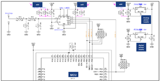
For the Vref and Vbd parts

It is improved by adding capacitor capacitance.

1)Is the approach that it is improved by changing capacitance value and voltage value of Vref correct?

2)It says "The analog power supply must always be greater than or equal to the digital power supply." in the datasheet.

Is the following combination acceptable?

Analog power +VA=5 V±1% (4.95~5.05 V), Digital power +VBD=5 V±1% (4.95~5.05 V)

Best Regards,

Ryusuke

  • Hello Ryusuke, 


    Thank you for your question.  It seems like the lower bits becoming biased sounds like a possible noise concern and improving the capacitance of the supplies and VREF is a great way to mitigate that (this is also part of the “Do’s and Don’ts” on section 10.3 of the datasheet)


    To answer your 1st question:

    Although adding 2x 4.7µF capacitors on the “+5VA” would certainly help I would like see the extent of the possible change. Has this schematic been built yet? Or is there still time to make more modifications? If the latter, to what extent can this be? 

    In the section 10 (Applications and Implementation), it covers some information on driving the reference. If possible, I would suggest looking into possibly having a reference driver.

    If a simpler approach is needed or preferred I would like to suggest changing C102 on your schematic to a 10 µF capacitor and adding a 0.1 µF decoupling capacitor for REF pin, with the decoupling capacitor as close to the pin as possible.  If some additional passive filtering can be added that would also be helpful (similar to the suggestion on the “Applications and Implementations” section).  

    Keeping C101 and C14 for the +VA pin would be a good idea.

    Another thing I wanted to ask regarding your concern with some of the possible noise is the driving circuit for your inputs, is there additional circuitry besides the two filters to drive the inputs? What kind of input signal is expected in this system? Could you share any more information of regarding your system?

    An input driver and kick-back/aliasing filtering is recommended for optimal performance. The other thing to note here is the output impedance of the two input pins should be matched to avoid offset error, gain error, and linearity errors that could also be causing the lower 3-bit biasing.  Section 10.1.2 in the datasheet would be helpful for this.


    For your 2nd question:

    Yes, having both +VA and +VBD set to 5V would be acceptable, this keeps both supplies within the recommended operating conditions as well as it complies with +VA≥+VBD requirements.    


    Best regards,

    Yolanda