This thread has been locked.

If you have a related question, please click the "Ask a related question" button in the top right corner. The newly created question will be automatically linked to this question.

ADS127L18: Check Block Diagram

Part Number: ADS127L18

Tool/software:

Hello experts, 

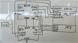
Would it be possible to check my thinking on the implementation of the ADS127L18 ADC through a block diagram?

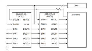
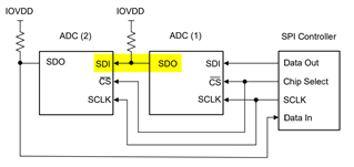
Essentially, we're daisy chaining 2 ADCs together and interfacing with one of them (let's call it #1) through McBSP. However, this is the part I'm concerned about: we want to use McBSP in SPI mode for the initial configuration of registers, while switching back to normal McBSP operation for reading data. Since MDR is the only pin that overlaps between the two protocols, we are using a demux to switch between the two modes. I am only worried about the digital side, so the analog part is not shown. Could you let me know if you think this setup will work, and, if not, why? Sorry if the photo is unclear, I'll gladly answer any questions you have. 

Thank you, 

Dylan

  • Hello Dylan,

    You setup should work, except the SDO of #1 should connect to SDI of #2 for proper daisy-chain of SPI control. 

    Since most processors have several dedicated SPI ports, I would suggest using a dedicated SPI port for this instead of trying to multiplex one of the McASP inputs.  The SPI is only used to read and write configuration registers, and does not need to be a high speed interface.  In fact, you could bit-bang (software SPI) using GPIO pins on the processor if you do not have a free SPI port to use.  However, if you want to add an external switch, then your approach will work as well.

    Regards,
    Keith Nicholas
    Precision ADC Applications