This thread has been locked.

If you have a related question, please click the "Ask a related question" button in the top right corner. The newly created question will be automatically linked to this question.

ADS1258: ADS1258 Channel Data Read Direct Questions

Part Number: ADS1258

Tool/software:

Hi,
I am working on the ADS1258 and I have questions about the Channel Data Read Direct command.

First, I am sending a register write command (the first three bits are "011"=Register Write Command) in order to configure the SINGLE-ENDED inputs I want to be active (making register MUXSG0 and MUXSG1 ="00000001"... which means I want Channel AIN0 and AIN8 to be active) this having the Multiple Register Access MUL='1'

Then I am sending a Channel Data Read Direct (first three bits of the command="000") in order to start reading converted data of the channels I just configured... Here, in the reading logic I have /DRDY present to start getting the data, and I can see that in effect in the STATUS byte it shows that it is switching between the two channels that I configured in writing, but I am reading the same data in both channels (here I only have an input signal in one of the pins that I configured, but the conversion appears in both channels), so in one of the channels DOUT should be '0's

I also set START pin as HIGH when /DRDY sets as LOW, and I send 32 cycles of SCLK for SPI. I attached the next figures showing that in first instance I am getting data from one of the configured channels and in the next /DRDY I get the next configured channel
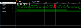
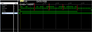
I still don't understand what is happening if I am configuring the reading taking into account /DRDY 
  • For update, the START signal seen in the image is a signal used for the SPI, but the START for the ADC is a signal that set as HIGH and stays that way

  • Hi Juan B,

    I don't think I fully understand your question: you are saying that the data is same for both channels, but in the images you provided the data is different between CHID 01000 and CHID 10000. So what is the issue? It would help to see images of when the data is "bad" versus when the data is "good"

    In single-ended mode the channels are measured with respect to the AINCOM pin - what voltage do you have applied to this pin?

    -Bryan

  • Hi Bryan,

    First of all thanks for replaying!

    You are right, the data is different between CHID, but the thing is that in the MISO signal I am getting data (the 3 bytes of data) in the CHID where I have an input signal set to off (AIN8 -> CHID="10000")

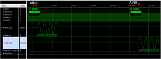
    Here is more explanation about the problem I have... According to the CHID I am filling a FIFO with the objective of collecting a certain amount of data (so I have 2 FIFOs, one for each CHID) and when it is already full and downloaded you can see how the signal of both FIFOs seems to be the same with a slight Delay or Phase Shift, as can be seen in the attached image, I mean that they are not the same but they keep the same form, but remember that one of the AINs is connected to an input signal off. So apparently, since the MISO signal for both CHID sends converted data, internally in the ADC what enters through AIN0 is taken as if it were entering in the same way through AIN8

    And with respect to AINCOM pin, it is grounded

  • Hi Juan B,

    What is connected to the channel that is "off"? I believe you have a voltage connected to AIN0, but it is not clear what is happening with AIN8?

    Can you provide a schematic of your system, as well as describe in detail how the inputs are being driven? Maybe a picture of your setup would help

    If you apply some other voltage to AIN8, does that voltage get read correctly?

    -Bryan

  • Hi Bryan,

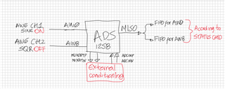
    I am working with a 2-Channel AWG, so one AWG channel s connected to AIN0 and the other AWG channel is connected to AIN8. I configure in the AWG channel 1 as a Sine signal an I turn the output ON, and the AWG channel 2 as a Square signal but the output is tuned off... Here I attach an image showing the path I am using for this to

    Here I am using EXTERNAL MULTIPLEXER LOOP (stting bit BYPAS='1' in CONFIG0 register) so the ADC converts what the extarnal conditioning is sending back (via ADCINP and ADCINN)... I think the problem is that the signal that the ADS1258 is sending (via MUXOUTP and MUXOUTN) is not being refresh and always takes the signal for AIN0

    Here I read in the datasheet about the Swtich TIme Delay (configured in bits DLY of CONFIG0) but I am not sure if the problem is solved this way

  • Hi Juan B,

    Can you try measuring purely DC voltages as a troubleshooting step. This will eliminate the AWG as a source of error and simplify your system:

    • Apply 1V (or some other nonzero voltage) to AIN0. This voltage is relative to GND/AINCOM
    • Apply 2V (or some other nonzero voltage that is different from AIN0) to AIN8. This voltage is relative to GND/AINCOM

    You can do this with AA batteries (so maybe you apply 1.5V and 3V then) if you don't have a precision DC source. Now you know exactly what you should be getting on each measurement. Please take 1000 samples (500 on each channel), and then report back the results in an excel file

    Please also send your ADS1258 register settings as well as a schematic of your system. I would like to see how you have connected the reference, clock, and the signal conditioning circuitry between MUXOUT/ADCIN

    -Bryan

  • Hi Bryan

    Sorry for the time I took to respond
    I performed the tests applying DC signals to the AIN inputs and analyzing every detail I discovered that the problem is directly in the hardware I am using...
    So for now the way forward is that I am going to do analysis and changes probably in hardware to find the solution to this problem
    Anyway, I really appreciate the help

  • Hi Juan B,

    Thanks for the update

    -Bryan