This thread has been locked.

If you have a related question, please click the "Ask a related question" button in the top right corner. The newly created question will be automatically linked to this question.

ADS1234 Data rate problem

Other Parts Discussed in Thread: TPS3836, ADS1234

I've post this writing in an old thread but think it is not coherent, so I'm posting it in a new thread.

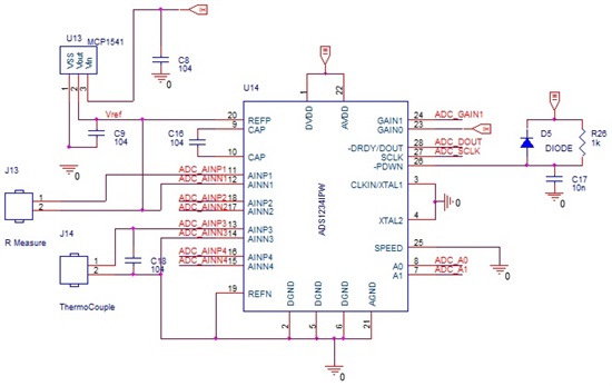
I'm using ads1234 and see its operation is weird. I did connect the part as follow: both XTAL1 and XTAL2 to 0V, SPEED to 0V,t PWDN to VDD via RC network (1kOhm and 10nF), all digital pins (SCLK, GAIN1, GAIN0, A1, A0) go to 0V.

As I see waveform on DRDY/DOUT pin on my ossiloscope, the pin pulse low to high to low every 11ms, pulse width is 4.2 us. I suspect this is 80 SPS mode but the hardware is in 10 SPS mode? The results retrived from adc is random and unstable. As I turn on and off the board, sometimes (about 10% of all cases), the pin pulse low to high to low every 100ms and the result is correct.

I don't know why the ic operation mode changes and the result is incorrect. Could you please help me on this issue? Thanks a lot.

Best regards,

T.anh

  • T.anh,

    Welcome to the forum!  I deleted your previous post so that anyone that may want to follow will not be confused.  It seems to me like you have a connection issue.    The SPEED pin may have a poor connection to ground.  How have you connected your system together?  Is it on a prototype PCB, solderless breadboard or some other prototyping method?  Can you send me a schematic of your setup?

    Perhaps you have an issue with grounding in general.  Is AGND and DGND connected?  There must be a very low impedance connection path between AGND and DGND.

    Best regards,

    Bob B

  • 1200.Bot Layer.pdf

    3377.Top Layer.pdf

    Mr Bob, thanks for your quick reply.

    I designed a 2-layer PCB for my project and just used copper poured ground, not a seperate ground layer. I attach here the schematic and layout of the board.

    AGND and DGND are all connected to 0V. I'm not sure if the impedance is low enough, how low is needed? Also, I don't think the incorrect results are caused by grounding because I didn't get any stable bit in them, all 24 bits change with time.


  • T.anh,

    Thanks for the detailed information.  The system should work for you.  At this point I would suspect a cold solder joint at pin 25.  Sometimes adding a little flux and reflowing the solder at the pin is all that is needed to correct the problem.

    Best regards,

    Bob B 

  • Mr Bob, I've resoldered the pin 25 as you said, I also check the connection with a multimeter, it is okie, but the problem still appears. One thing changed is that the ic works in correct mode (10 SPS) more than incorrect mode. As I tried turning on and off the board and see the operation, 80% of cases the mode is correct.

    One more thing, when the mode is incorrect, if I reduce VDD  a bit (5.5V to 5.4V), the ic will turn to correct mode suddenly.

    Any suggestion about the error I'm facing?

  • T.ahn,

    Ok, now we have some information that wasn't in the schematic and that is the supply voltages.  You are exceeding the electrical specification of the supply voltages.  There are two specifications.  The first is the absolute maximum voltage that may be applied without damaging the part, and that is 6V for both AVDD and DVDD.  The second specification is the electrical characteristics to which the part will run properly.  This specification has a minimum and a maximum voltage.  This range is shown in the table on page 4 of the datasheet under Power Supply.  The minimum is 2.7V and the maximum is 5.3V.  So 5.5V is too high, and so is 5.4V.  This applies to both AVDD and DVDD.

    Best regards,

    Bob B

  • 5.5 and 5.4 V are just levels I used to seek for the cause of the problem (eg. I fluctuate VDD back and forth to see if it relates someway to the problem). My VDD is fixed at 5V and the ic still works in wrong mode about 20% of all cases!

    As it is in the wrong 80 SPS mode, if I reset it (by pulling down PWDN pin), it returns to correct 10 SPS mode afterwards.

    Could you give me any suggestions?


  • The only solution I'm using is to keep control of PWDN pin using my microcontroller, not rely on RC network more. As I pull high this pin 1s after turn on the board, the problem is solved.

    But about the root of it, I don't understand.

  • T.ahn,

    I'm sorry that I didn't catch this earlier.  Your RC values are incorrect.  You need at least a 2.2nF cap at the power down pin.  Note page 23 of the datasheet and the Power-up Sequence section and the figures 39 and 40.  There must be a minimum of 10us from AVDD fully high and the PDWN pin going high.  With the shorter delay time the power up reset conflicts with the reset that happens with the PWDN pin going high.  This places the device in a conflicted state.

    Best regards,

    Bob B

  • Hello sir,

    Can i connect 18pf capacitor on below mention pin???

    (((You need at least a 2.2nF cap at the power down pin.  Note page 23 of the datasheet and the Power-up Sequence section and the figures 39 and 40)))


    Regards,

    Jignesh..

  • Hi Jignesh,

    There are a lot of ways you can hold the device in the power down state.  What is important here is that the power down state holds the device in reset until the device is completely powered.  If DVDD is powered first and then AVDD, you must make sure that the AVDD supply has been completly powered for at least 10us before the PWDN pin is brought high.  This will ensure that a proper power on reset has taken place. 

    Figure 40 shows a known working RC circuit.  If you lower the value of C, you must also increase the value of R so that the time constant remains the same or longer. 

    Another approach would be to set the PWDN pin state with the microcontroller used for communication.  I would use a pull-down resistor on the PDWN pin (also connected to the micro) to make sure that the pin is held low while the micro powers up.  Hold the pin low using the GPIO of the micro until the prescribed time and then pull the pin high.

    A third approach would be to use a supervisor logic circuit that will hold the pin low for a predetermined amount of time.  An example would be the TPS3836 and family of devices.

    Best regards,

    Bob B

  • Thanks Bob,

    I will try as per suggestion and give feedback,

    Regards,

    Jignesh

  • Hello Sir,

    Good evening..

    I am using PIC16F877A microcontroller with ADS1234.

    I tried your suggested both option, but I can't get DRDY Pin Low in any condition.

    I also replace ADC but same result as, not get.

    I also short Crystal both pin to Ground but same result as, not get.

    what exastly problem I can't understand?

    pls let me suggest test procedure of ADS1234 in sequence.... what I do??

    Is there SPI module enable require in micro controller?/

    I attached herewith my schematic..

    Pls help.

    Jignesh

  • Hi Jignesh,

    I think the best thing to do at this point is to replace R5 and R6 (4.7k resistors) with 0 ohm (direct short).  There should be a low impedance connection between the AGND and DGND of the ADS1234.  Also, you will starve the analog portion of the device by restricting the current to AVDD.  If you want to add some filtering, try 10 ohms at AVDD, but in no way should you add any resistance between the grounds.

    Best regards,

    Bob B

  • Respected Sir,

    sorry for the wrong value(by mistake) in the schematic, correct value of R5 and R6 are 0 ohm, I think all condition of my side is good as per schematic.

    I done following configuration from schematic...

    my ADC configuration is,

    I connect PWDN to microcontroller with Pull Down Resistor.

    VDD =+5V, AVDD =+5V,

    A0=0, A1=0,

    SPEED=0,

    GAIN0=1, GAIN1=1,

    but I can't understand what exact problem?

    my again same question,,, 

    pls let me suggest test procedure of ADS1234 in sequence.... what I do??

    Is there SPI module enable require in micro controller?/

    Regards,

    Jignesh..

  • Hi Jignesh,

    This part is really not hard to use as all the configuration is by pin control.  Follow this order for startup of ADS1234 (this is assuming that you have setup the microcontroller correctly -- and yes you do need to setup the micro for SPI peripheral):

    • Apply power to the ADS1234 (both AVDD and DVDD) and make sure both are present at the device.
    • Wait at least 10us after AVDD power is applied and settled to full value, then set the PWDN pin high.
    • Check that the crystal is oscillating (if you use the crystal, otherwise tie the XTAL1 pin 3 low).
    • Check DOUT/DRDY pin and it should pulse at about every 100ms with SPEED low.

    Do not connect pull-ups or pull-downs on the DOUT/DRDY signal as there is no need to do so.  Also, do not connect pull-ups and pull-downs at the same time to the digital inputs to the ADS1234.  I would suggest that based on the configuration you have mentioned to place pull-downs on A0, A1, PDWN, and SPEED, and pull-ups on GAIN0 and GAIN1.

    Also, I can't tell if you have used the correct pins for your schematic symbol as the picture is not clear enough to show me the detail to read the pin numbers.  Make sure your symbol matches precisely with the datasheet pins.  Also make sure that the footprint you are using for the PCB also matches correctly.

    Best regards,

    Bob B

  • Hello Sir,

    Good Morning. Thanks for support.

    I done everything as per your suggestion, but i can't got low in DRDY pin.

    I tell you one thing,, can I test ADS1234 without microcontroller... not require data but only I wish to see DRDY pin low.

    pls help.

    Thanks and Regards,

    Jignesh

  • Hi Jignesh,

    The ADS1234 is a pin controlled device, so the only thing you need the microcontroller for is to read the data out from the device.  If power is supplied to the device, and if the digital pins are configured properly, you should see the DOUT/DRDY pin transition at the selected data rate.  This also requires that the CLK is working properly.  If you use an external crystal you must make sure that it starts to oscillate at the specified frequency.  If it does not, then there may be an issue with the capacitor loading or PCB layout with the oscillator circuit.

    It is best to try and use the internal oscillator first by connecting the CLKIN pin to ground.  You must do this prior to powering the device.  In other words the internal oscillator will shut down if noise or another signal is on the CLKIN pin after startup.  If there is no CLK, then the device will not work at all and will behave in the manner you are describing.  I suspect there is an issue with the CLK in your setup.

    Best regards,

    Bob B