This thread has been locked.

If you have a related question, please click the "Ask a related question" button in the top right corner. The newly created question will be automatically linked to this question.

ADS131M02: Data Ready Interrupts do not occur at the right frequency

Part Number: ADS131M02
Other Parts Discussed in Thread: AMC131M02,

Tool/software:

Hello,

I am able to successfully read the ADC values. However, I'm not seeing the correct data rate frequency as mentioned in the datasheet. Here's some background on my setup.

I have the CLKIN frequency set to 5.102MHz. The idea behind choosing this clock was to sync the data rates to an ISR we have that's running at 39.86KHz. The formula in the datasheet for the data rate with an OSR of 64 is:
Data rate = (CLKIN / 2 * OSR) = (5.102 / 2 * 64) = 5.102 / 128 = 39.86Ksps. 

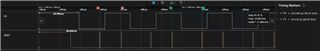
However, we see the DRDY interrupts occur very haphazardly. I see the first interrupt come in at 95.31KHz and the second at 68.87KHz, and this pattern repeats. The ADC is set to 16-bit mode and 64 OSR correctly. 

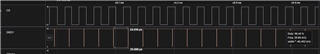
However, if I change the OSR to 128, and set the DRDY_FMT bit to 1 or 0, the interrupt occurs at my desired frequency correctly:

So is the data rate actually = CLKIN / OSR? Please clarify. Am I doing something wrong here?

  • Hi Dheera,

    Your calculation for the output data rate is correct. The difference between these timing diagrams you shared is your /CS in the 1st timing is kept low after the next /DRDY pulse arrives. Do you read data from the ADC by checking the falling edge of the /DRDY?

    BR,

    Dale

  • Hi Dheera,

    I also want to add a few additional details.

    The DRDYn pin indication is "blocked" while you are reading conversion data. I assume you are reading the conversion data in your first diagram. That is why you see the DRDYn pin high-low transition after you read out the data from both ADC channels.
    Ideally you should read out conversion data before the next conversion result completes. In your first diagram you are reading data slower than the conversion period.

    I would also like to point you to the description of the DRDYn pin behavior which is currently only described in the AMC131M02 datasheet in the "8.5.4 ADC Output Buffer and FIFO Buffer" section. We will add this information to the ADS131M02 datasheet in the next revision as well.

    Regards,
    Joachim Wuerker

  • Sorry for the delay in response. We were trying to probe the CLKIN to make sure it was right. Looks like it was 2x the frequency (5.102 * 2 = 10MHz). 

    That explains the data rate being twice. Once we fixed it, the data rate behaves as expected. Thanks for your help as always.

    Regards,
    Dheeraj