This thread has been locked.

If you have a related question, please click the "Ask a related question" button in the top right corner. The newly created question will be automatically linked to this question.

DAC61416: Assistance Required for DAC61416 Configuration in Varactor Diode Biasing Circuit

Part Number: DAC61416
Other Parts Discussed in Thread: LM25116, LM5116, LM5088, LM25088, LMZM33604, TPSM63608

Tool/software:

Dear TI Team,

We are in the process of designing a circuit that requires an analog voltage range of 0 to -12V to bias 256 varactor diodes in the reverse voltage region. After evaluating options, we have selected the DAC61416 for this purpose. However, we would like to clarify a few technical details:

  1. Power Supply Requirements:

    • To achieve an output range of 0 to -12V, could you please confirm the appropriate values for VCC, VSS, VDD, and VAA?
  2. SPI Daisy-Chaining DACs:

    • Given that we need to bias 256 varactor diodes, we plan to use 16 DAC61416 devices. Could you provide guidance on the best approach to daisy-chain SPI interface for these DACs when interfacing with a microcontroller?
  3. Additional Circuitry:

    • Are there any additional circuits, such as buffers or amplifiers, that you would recommend for conditioning the DAC output before applying it to the varactor diodes?

Attached is a high-level diagram of our design for your reference.

We appreciate your support and look forward to your guidance on these questions.

Best regards,
Meghla

  • Hi Meghla,
     
    Please check my response below for each of the queries.
     

    • Power Supply Requirements:

      • To achieve an output range of 0 to -12V, could you please confirm the appropriate values for VCC, VSS, VDD, and VAA?
        - VCC = +9V (min) or greater than this, VSS = -13.5V (max) or less than this, VDD = VAA = 5V
        -  (VCC - VSS) <= 43V
    • SPI Daisy-Chaining DACs:

      • Given that we need to bias 256 varactor diodes, we plan to use 16 DAC61416 devices. Could you provide guidance on the best approach to daisy-chain SPI interface for these DACs when interfacing with a microcontroller?
         - Let me check this for you and will get back to you.
    • Additional Circuitry:

      • Are there any additional circuits, such as buffers or amplifiers, that you would recommend for conditioning the DAC output before applying it to the varactor diodes?
         - No, this devices already have a internal reference and output buffers.
         - I would be able to comment better if you can provide the load current and voltage accuracy requirements for varactor diode, if there is any.

     
    Thanks,
    Sanjay

    • We are considering the following two options for the power supply configuration:

      • Option 1: VCC = 12V and VSS = -12V
      • Option 2: VCC = 12V and VSS = -13.5V

      We would prefer Option 1 if it is possible to design with these voltages. Could you confirm if this is viable and explain how these voltage values are being selected? Additionally, could you provide guidance on the necessary voltage headroom for this configuration?

      Also, what should be the voltage of VIO in this setup?

      Lastly, could you share any calculations related to the power dissipation and consumption for the DAC61416 under these conditions?

      2. Additional Circuitry:

      We understand that the DAC61416 has an internal reference and output buffers, but we would like to confirm if any additional circuitry (e.g., external buffers or amplifiers) is needed for conditioning the DAC output before applying it to the varactor diodes.

      For reference, our application has the following requirements:

      • Load current per varactor diode: ~50nA
      • Voltage accuracy required: ±0.01V

      Thank you for your support. We look forward to your guidance on these points.

  • Hi Meghla,
     
    Please check my response below for each of the queries.
     

    • SPI Daisy-Chaining DACs:

      • Given that we need to bias 256 varactor diodes, we plan to use 16 DAC61416 devices. Could you provide guidance on the best approach to daisy-chain SPI interface for these DACs when interfacing with a microcontroller?
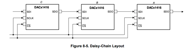
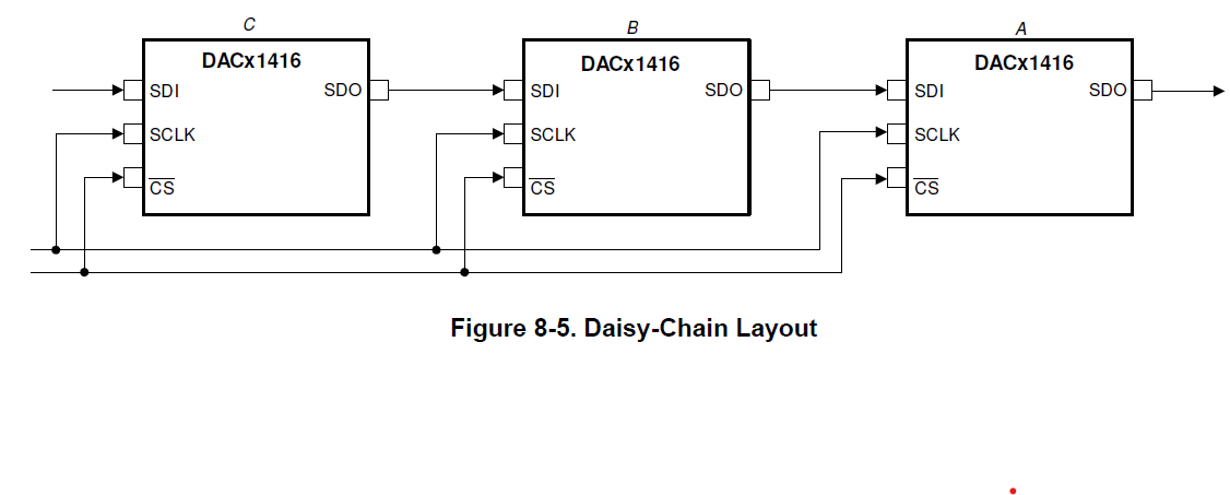
         - You can connect any number (N) of devices in daisy chain method. Please check the sample diagram below.
    • Power Supply Requirements:

      • Option 1: VCC = 12V and VSS = -12V
      • Option 2: VCC = 12V and VSS = -13.5V
         - Go for the Option 2 as you need the foot room voltage for VSS. Earlier i had considered worst case condition and provided you the 1.5V foot room w.r.t. VSS power supply. Please check the plot below for head/foot room voltage w.r.t. required load current
           

      • Although you can reduce the supply voltage as low as VSS = -12.1 V (0.1V foot room) as your current requirement is only 50nA.
      • VIO can be anything between 1.7V to 5.5V
      • Power dissipation (typical case and ignoring the load current as it's 50nA only) - 
        - for current source >> Pd = (VCC - VOUT) * I(VCC) = ~ (12.0 - (-12.0)) * 10 mA = 0.24 W
        - for current sink >> Pd = |(VSS - VOUT)| * I(VCC) = ~ |(12.0 - (-13.5))| * 10 mA = 0.015 W
      • Power dissipation (worst case and ignoring the load current as it's 50nA only) - 
        - for current source >> Pd = (VCC - VOUT) * I(VCC) = ~ (12.0 - (-12.0)) * 25 mA = 0.6 W
        - for current sink >> Pd = |(VSS - VOUT)| * I(VCC) = ~ |(12.0 - (-13.5))| * 25 mA = 0.0375 W
    • Additional Circuitry :

      • Load current per varactor diode: ~50nA
      • Voltage accuracy required: ±0.01 V

         - Total error from the DAC (typical case) = % TUE Error * voltage range span / 100 
                                                                          = 0.01 % x 40V / 100 = 4mV 
         - Total error from the DAC (worst case) = % TUE Error * voltage range span / 100 
                                                                          = 0.1 % x 40V / 100 = 40mV 
      • It means, you can go ahead for 0.01 V error target if this is not a very stringent requirement. Otherwise you will need offset correction at the output of the DAC channels.


    Thanks,
    Sanjay

  • Hi Sanjay, 

    Thanks for the replies. 

    1. SPI daisy chain: If we operate at highest clock speed for  SPI communication then how many devices can we connect in daisy chain method ? 

    2. Could you please suggest good efficiency  DC -DC converter from TI for 12V -5V (1A output current) and 12V- -13..5V (1A output current)  for this application ?

    Thanks & Regards,

    Meghla

  • Hi Meghla, 

      
    1. SPI daisy chain: If we operate at highest clock speed for  SPI communication then how many devices can we connect in daisy chain method ? 
     - Max clock speed that you can use would be 
         - 25MHz for 1.7V < VIO < 2.7V 
         - 25MHz for 2.7V < VIO < 5.5V 
         * Please refer to the section 7.6 Timing Requirements of the DAC81416 data sheet for more details.

    2. Could you please suggest good efficiency  DC -DC converter from TI for 12V -5V (1A output current) and 12V- -13..5V (1A output current)  for this application ?
     - I would suggest you to use the TI's  DC/DC power designer tool webench. You just have enter the inputs and It will give you multiple option to choose from. And further you will get the design, BOM/part# and simulation option. 
    webench designer tool link - webench.ti.com/.../switching-regulator


    Let me know if need any more help.
     
    Thanks,
    Sanjay

  • Hi Sanjay,

    I recently explored the WEBENCH® POWER DESIGNER by Texas Instruments, and I found it to be an incredibly useful tool for designers. I have a couple of queries that I hope you can help me with:

    1. For our application, we need to convert a 12V input voltage to a 5V output voltage with a 1A output current. What Vmin and Vmax values should I input into the tool to find the appropriate DC-DC converter for this application?

    2. Similarly, for the configuration converting 12V input to -13.5V output, what should be the recommended Vmin and Vmax values to input in the tool?

    Thank you for your assistance.

    --

    Regards,

    Meghla

  • Hi Meghla, 


    Vin min-max are for - 

    a. in case target application has variable supply
    b. supply has noise, error or ripple (typically from DC/DC modules) 

    For your case, you can consider Vin = 12V +/- 1V (just giving you worst case number) as you have fixed supply Vin = 12V.


    Thanks,
    Sanjay

  • Hi Sanjay,

    We have a couple of queries regarding the schematic design of the DAC61416:

    1.  DC Voltage Generation:

      • Using the Webench TI Power Designer, we selected the TPS563252DRLR for generating 12V to 5V DC.
      • For generating 12V to -13.5V DC, the TI Power Designer suggested using inverting buck-boost converters such as LM25116, LM5116, LM5088, and LM25088. However, the datasheets for these parts do not explicitly mention support for negative or inverting voltage outputs. While the LMZM33604 supports inverting applications, its 16x10mm size does not fit our requirements.
      • Could you please confirm if there are any other smaller-sized inverting DC-DC buck regulators that can generate -13.5V from 12V?
    2. DAC61416 Toggle Registers:

      • The datasheet mentions that Toggle 0, 1, and 2 can be connected to configure toggling between DAC Register A & B. Could you please explain in which scenarios or applications toggling between these two registers is necessary, and when we would need to use this feature?

    Regards,

    Meghla

  • Hi Meghla, 


     1. You can try out the TPSM63608 for this application 
         Data sheet - 9.2.2 Design 2 – Inverting Buck-Boost Regulator with Negative Output Voltage
         
       Note - I have limited knowledge on power related products, I would request you to please refer power design related questions to the power management team on E2E. 

     2. Toggle feature enables to have DAC output switching between two values just using the HW or SW toggle feature, without having to write teh DAC data via SPI command. You can use the toggle feature to generate a square wave, ON/OFF signal or any other waveform as per toggle input. I would request you go to g through the toggle mode section 8.4.1 Toggle Mode in data sheet.
     

    Thanks,
    Sanjay

  • Hi Sanjay,

    We have completed the schematic for the DAC61416. Here are a few additional questions we have:

    1. What is the difference between RESET and CLR functions?
      We’d like to clarify the distinct roles of the RESET and CLR functions. Specifically, could you provide details on how each function affects the DAC outputs and registers?

    2. Retention of Configuration Values Post Power-On Reset
      After a power-on reset, will the DAC retain its previously configured values, or will it require reconfiguration? Additionally, when we want to change the output values, which function—RESET or CLR—should we use to reset the output values without losing other configurations?

    3. Synchronous Mode Operation for Biasing 256 Antenna Elements
      Our application involves biasing 256 antenna elements with unique voltages using the DAC outputs. Would you recommend synchronous mode operation for this application, or would another configuration be more suitable to achieve consistent and stable outputs?

    4. Schematic Review
      We have attached the DAC61416 schematic. Could you please review it and confirm if it aligns with the design specifications, or let us know if there are any changes required?

  • Hi Meghla,

    Please check my response against each query below:

    1. What is the difference between RESET and CLR functions?
      We’d like to clarify the distinct roles of the RESET and CLR functions. Specifically, could you provide details on how each function affects the DAC outputs and registers?
       - RESET : RESET [HW or SW] initiates a POR event. For more details, refer to the data sheet.
       - POWE ON RESET (POR) : The DACx1416 includes a power-on reset function. After the supplies have been established, a POR event is issued. The POR causes all registers to initialize to their default values and communication with the device is valid only after a 1-ms power-on-reset delay. After a POR event, the device is set in power-down mode where all DAC channels and internal reference are powered down and the DAC output pins are connected to ground through a 10-kΩ internal resistor.
       - CLR : This action sets the DAC code inn such a way that output voltages becomes 0V. Details are in the data sheet section 8.3.1.2.3 Clear DAC Operation

    2. Retention of Configuration Values Post Power-On Reset
      After a power-on reset, will the DAC retain its previously configured values, or will it require reconfiguration? Additionally, when we want to change the output values, which function—RESET or CLR—should we use to reset the output values without losing other configurations?
       - POR will reset the device to default state. Use CLR pin if you want to clear the DAC output code setting only and retain the other settings.

    3. Synchronous Mode Operation for Biasing 256 Antenna Elements
      Our application involves biasing 256 antenna elements with unique voltages using the DAC outputs. Would you recommend synchronous mode operation for this application, or would another configuration be more suitable to achieve consistent and stable outputs?
       - it does not matter if you use synchronous mode or asynchronous mode. Once DAC output is set to a voltage, it will stay on that voltage unless you change the DAC code or do something else.

    4. Schematic Review
      We have attached the DAC61416 schematic. Could you please review it and confirm if it aligns with the design specifications, or let us know if there are any changes required?
       - What is the min/max impedance [inductor + diode] seen by the DAC output in operating condition? If it's very low, please add biasing resistor in series for each channel.
       - Use 0.1uF decap for VIO power pin.
       - Rest of the things are okay. 

    Thanks,
    Sanjay

  • Hi Sanjay,

    Thanks for the replies. 

    4. Schematic Review: In our application output voltages at DAC will vary from -0.5V to -12V. so we have directly connected the DAC outputs to varactor diodes. 

    --

    Regards,

    Meghla

  • Hi Meghla,

    Then this should be okay. I would still suggest to add the biasing resistor just for design robustness, and that you can decide.

    Thanks,
    Sanjay 

  • Hi Sanjay,

    Thank you for your response.

    We have a few additional questions regarding the daisy-chain configuration of the DAC61416. Based on our interpretation of the datasheet, we believe the update sequence might work as follows:

    1. In the initial 24 clock cycles, Channel 0 of DAC C (the first DAC in the chain) is updated.
    2. In the following 24 clock cycles, the configuration moves to the next DAC in the chain to update its Channel 0.
    3. This pattern would then continue, updating Channel 0 of each DAC in 24 x N clock cycles (where N is the DAC number in the chain).
    4. Once all DACs’ Channel 0 values are updated, we would then select the next channel register address to repeat the process for Channel 1 of each DAC.
    5. Subsequently, Channels 2 through 16 would be updated across all DACs in the daisy chain following the same pattern.

    Alternatively, we’d like to confirm if, in a daisy-chain configuration, all channels of DAC 1 are configured first, and then through the SDO pin, we configure all the channels of the subsequent DACs one after another.

    Could you please confirm which of these configurations is correct?

    Thank you for your assistance

  • Hi Meghal,
     
    It's not exactly correct, here is how daisy chain works - 
     
    >> SDO is by default enabled and it should not be disabled.
    >> Each 24 bits of a frame corresponding to a command is independent to each other and need not to be same in a single daisy chain operation.
    >> First CSz lows low
    >> If you look at diagram below, for 3x 24 bit frame 
         - first 24 bits go to device A, 
         - next 24 bits go to device B, 
         - fanal 24 bits go to device C,     
    >> and these 3x24 bits data will not be honoured by any of device A, B or C, until the CSz goes high.  
    >> Before CSz goes high, data will reside in the device but wouldn't be activated. It happens only after CSz high operation.
     
    Again as I said earlier, each 24 data set can be same or independent within a single daisy chain frame (for this case 3x24 bits of data). It's upto you how you want to configure each device. Even though A, B and C are connected in a chain, you can still perform independent  write operation for each device.
     
    Thanks,
    Sanjay


  • Hi Sanjay,

    Thank you for the detailed explanation.

    We understand now how the data updates occur for Channel 1 across DACs A, B, and C in a daisy-chain configuration. To confirm our understanding, when updating Channel 2, does the sequence continue by selecting the next register in DAC A, B, and C, and so forth through all 16 channels of each DAC, one at a time?

    We’d like to confirm if our interpretation is correct, that each channel is updated sequentially across all DACs in the chain, following the same pattern as the first channel.

    Thank you again for your guidance!

    Regards,

    Meghla

  • Hi Meghla,

    I have dropped a mail on your registered e-mail ID. Please check there and respond.

    Thanks,
    Sanjay