ADS1299: Regarding the impedance matching of PCB boards

Part Number: ADS1299

Tool/software:

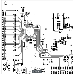
I plan to use ADS1299 to design a PCB acquisition board for collecting EEG signals. I want to know the impedance between the electrode and the channel pin of ADS1299, as well as the impedance in other places. My main goal is to achieve impedance matching. Design PCB routing parameters such as line width and copper thickness based on the required impedance. So how can I determine the impedance required for ADS1299.For example, what is the impedance of the PCB board diagram in the design manual of ADS1299EEG-FE below? And what is the line width?

  • Hello Di,

    The trace width and impedance information is not available for the ADS1299 EVM. 

    For low-frequency applications, absolute trace impedance and impedance matching is not really necessary as it may be in high speed DAQ or RF applications. Care should be taken to route the electrode input paths as symmetrically as possible to minimize offset due to leakage current. Proper ground shielding and differential/common-mode filtering are more important design considerations since ambient noise coupling is generally a concern in such bio-potential applications.

    Regards,

    Ryan