This thread has been locked.

If you have a related question, please click the "Ask a related question" button in the top right corner. The newly created question will be automatically linked to this question.

ADS1220: Issue with Configuration and Inconsistent Raw Data Readings

Part Number: ADS1220


Tool/software:

Dear TI Community,

I am currently working with the ADS1220 and facing some challenges with my configuration and data readings. Here are the details of my setup:

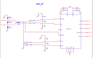
please do verify Schematic Diagram Two Wire RTD And please check my code .

Configuration:

  • Register 0: Command 0x66

    • AINp = AIN1,AINn = AIN0
    • Gain = 8
    • PGA = Enabled
  • Register 1: Command 0x04

    • Data Rate = 20 SPS
    • Normal mode
    • Continuous Conversion mode
  • Register 2:command 0x55h

  •        External Reference configuration(REFP0,REFN0)

    • Simultaneous 50Hz/60Hz rejection
    • IDAC = 500 µA
  • Register 3:command 0x80

  • IDAC1 connected to AIN3/REFN1

Procedure:

  1. I first send the command 0x06 (Reset Command).
  2. Before reading data, I send the command 0x08 (Start Conversion).

Issue:

I am using a PT100 RTD for temperature measurement, but the ADC raw data does not change with varying temperatures. I am only receiving two values: 8388351 and 8387839, regardless of the temperature applied to the RTD.

Questions:

  1. Is this issue likely related to hardware or software configuration?
  2. Are there any specific settings or steps I might be missing that could help improve the consistency of the readings?

I appreciate any guidance or suggestions you can provide.


Thank You!

  • please check my code   

    #ifndef INC_ADS1220_H_
    #define INC_ADS1220_H_

    #include "main.h" // Your project's main should include HAL

    //Commands
    #define ADS1220_RESET 0x06 // Good idea to reset on power-up
    #define ADS1220_START 0x08 // Both single-shot and continuous conversion must be started via 0x08
    #define ADS1220_WREG 0x40
    #define ADS1220_RREG 0x20

    //Registers
    #define ADS1220_CONFIG_REG0_ADDRESS 0x00
    #define ADS1220_CONFIG_REG1_ADDRESS 0x01
    #define ADS1220_CONFIG_REG2_ADDRESS 0x02
    #define ADS1220_CONFIG_REG3_ADDRESS 0x03

    //Masks
    #define ADS1220_REG_CONFIG1_DR_MASK 0xE0
    #define ADS1220_REG_CONFIG0_PGA_GAIN_MASK 0x0E
    #define ADS1220_REG_CONFIG0_MUX_MASK 0xF0

    //Sample rate
    #define ADS1220_DR_20SPS 0x00
    #define ADS1220_DR_45SPS 0x20
    #define ADS1220_DR_90SPS 0x40
    #define ADS1220_DR_175SPS 0x60
    #define ADS1220_DR_330SPS 0x80
    #define ADS1220_DR_600SPS 0xA0
    #define ADS1220_DR_1000SPS 0xC0

    //PGA gain settings
    #define ADS1220_PGA_GAIN_1 0x00
    #define ADS1220_PGA_GAIN_2 0x02
    #define ADS1220_PGA_GAIN_4 0x04
    #define ADS1220_PGA_GAIN_8 0x06
    #define ADS1220_PGA_GAIN_16 0x08
    #define ADS1220_PGA_GAIN_32 0x0A
    #define ADS1220_PGA_GAIN_64 0x0C
    #define ADS1220_PGA_GAIN_128 0x0E

    //Input mux
    #define ADS1220_MUX_AIN0_AIN1 0x00
    #define ADS1220_MUX_AIN0_AIN2 0x10
    #define ADS1220_MUX_AIN0_AIN3 0x20
    #define ADS1220_MUX_AIN1_AIN2 0x30
    #define ADS1220_MUX_AIN1_AIN3 0x40
    #define ADS1220_MUX_AIN2_AIN3 0x50
    #define ADS1220_MUX_AIN1_AIN0 0x60
    #define ADS1220_MUX_AIN3_AIN2 0x70
    #define ADS1220_MUX_AIN0_AVSS 0x80
    #define ADS1220_MUX_AIN1_AVSS 0x90
    #define ADS1220_MUX_AIN2_AVSS 0xA0
    #define ADS1220_MUX_AIN3_AVSS 0xB0

    #define Monitor_Bypass 0xC0
    #define AVDD_AVSS_Bypas_Negative 0xD0
    #define AVDD_AVSS_Bypass_Positive 0xE0

    #define _BV(bit) (1<<(bit))
    uint8_t cmd1=0x08;
    struct ADS1220_regs_s
    {
    uint8_t cfg_reg0; // = 0x00; //AINP=AIN0, AINN=AIN1, gain=1, PGA is enabled
    uint8_t cfg_reg1; // = 0x04; //20SPS, Mode=Normal, Conversion=Continuous, Temp mode disabled, Current source disabled
    uint8_t cfg_reg2; // = 0x10; //Internal 2.048V VREF, 50/60Hz filter, transistors open, IDAC off
    uint8_t cfg_reg3; // = 0x00; //IDAC1&2 are disabled, only DRDY signals conversion completion
    } ADS1220_default_regs =
    { 0x66, 0x04, 0x55, 0x80 };

    typedef struct ADS1220_regs_s ADS1220_regs; // Default init

    void ADS1220_writeRegister(SPI_HandleTypeDef *hspi, uint8_t address, uint8_t value)
    {
    uint8_t arr[2] =
    { ADS1220_WREG | (address << 2), value };

    HAL_GPIO_WritePin(GPIOE, GPIO_PIN_12,RESET);

    HAL_SPI_Transmit(hspi, arr, 2, 100);
    HAL_GPIO_WritePin(GPIOE, GPIO_PIN_12,SET);
    }

    uint8_t ADS1220_readRegister(SPI_HandleTypeDef *hspi, uint8_t address)
    {
    uint8_t data[2] =
    { 0, 0 };

    uint8_t txd[2] =
    { (ADS1220_RREG | (address << 2)), 0xFF };
    HAL_GPIO_WritePin(GPIOE, GPIO_PIN_12,RESET);

    HAL_SPI_TransmitReceive(hspi, txd, data, 2, 1000); // When doing bidirectional, transmit a dummy byte(0xFF), 2 in total, received register is in [1]
    HAL_GPIO_WritePin(GPIOE, GPIO_PIN_12,SET);
    return data[1];
    }

    void ADS1220_reset(SPI_HandleTypeDef *hspi)
    {
    const uint8_t cmd = ADS1220_RESET;
    HAL_GPIO_WritePin(GPIOE, GPIO_PIN_12,RESET);
    HAL_SPI_Transmit(hspi, (uint8_t*) &cmd, 1, 100);
    HAL_GPIO_WritePin(GPIOE, GPIO_PIN_12,SET);
    }

    uint8_t ADS1220_init(SPI_HandleTypeDef *hspi, ADS1220_regs *r)
    {
    ADS1220_reset(hspi);
    HAL_Delay(100);

    ADS1220_writeRegister(hspi, ADS1220_CONFIG_REG0_ADDRESS,r->cfg_reg0);//0x40
    ADS1220_writeRegister(hspi, ADS1220_CONFIG_REG1_ADDRESS, r->cfg_reg1);//0x04
    ADS1220_writeRegister(hspi, ADS1220_CONFIG_REG2_ADDRESS,r->cfg_reg2);//0x10
    ADS1220_writeRegister(hspi, ADS1220_CONFIG_REG3_ADDRESS, r->cfg_reg3);//0x00

    HAL_Delay(10);

    uint8_t CR0 = ADS1220_readRegister(hspi, ADS1220_CONFIG_REG0_ADDRESS);
    uint8_t CR1 = ADS1220_readRegister(hspi, ADS1220_CONFIG_REG1_ADDRESS);
    uint8_t CR2 = ADS1220_readRegister(hspi, ADS1220_CONFIG_REG2_ADDRESS);
    uint8_t CR3 = ADS1220_readRegister(hspi, ADS1220_CONFIG_REG3_ADDRESS);

    return (CR0 == r->cfg_reg0 && CR1 == r->cfg_reg1 && CR2 == r->cfg_reg2 && CR3 == r->cfg_reg3);
    }

    void ADS1220_start_conversion(SPI_HandleTypeDef *hspi)
    {
    // const uint8_t cmd = ADS1220_START;
    HAL_GPIO_WritePin(GPIOE, GPIO_PIN_12,RESET);
    HAL_Delay(5);
    HAL_SPI_Transmit(hspi, &cmd1, 1, 100);
    HAL_Delay(5);
    HAL_GPIO_WritePin(GPIOE, GPIO_PIN_12,SET);
    }

    void ADS1220_enable_PGA(SPI_HandleTypeDef *hspi, ADS1220_regs *r)
    {
    r->cfg_reg0 &= ~_BV(0);
    ADS1220_writeRegister(hspi, ADS1220_CONFIG_REG0_ADDRESS, r->cfg_reg0);
    }

    void ADS1220_disable_PGA(SPI_HandleTypeDef *hspi, ADS1220_regs *r)
    {
    r->cfg_reg0 |= _BV(0);
    ADS1220_writeRegister(hspi, ADS1220_CONFIG_REG0_ADDRESS, r->cfg_reg0);
    }

    void ADS1220_set_conv_mode_continuous(SPI_HandleTypeDef *hspi, ADS1220_regs *r)
    {
    r->cfg_reg1 |= _BV(2);
    ADS1220_writeRegister(hspi, ADS1220_CONFIG_REG1_ADDRESS, r->cfg_reg1);
    }

    void ADS1220_set_conv_mode_single_shot(SPI_HandleTypeDef *hspi, ADS1220_regs *r)
    {
    r->cfg_reg1 &= ~_BV(2);
    ADS1220_writeRegister(hspi, ADS1220_CONFIG_REG1_ADDRESS, r->cfg_reg1);
    }

    void ADS1220_set_data_rate(SPI_HandleTypeDef *hspi, int datarate, ADS1220_regs *r)
    {
    r->cfg_reg1 &= ~ADS1220_REG_CONFIG1_DR_MASK;
    r->cfg_reg1 |= datarate;
    ADS1220_writeRegister(hspi, ADS1220_CONFIG_REG1_ADDRESS, r->cfg_reg1);
    }

    void ADS1220_select_mux_config(SPI_HandleTypeDef *hspi, int channels_conf, ADS1220_regs *r)
    {
    r->cfg_reg0 &= ~ADS1220_REG_CONFIG0_MUX_MASK;
    r->cfg_reg0 |= channels_conf;
    ADS1220_writeRegister(hspi, ADS1220_CONFIG_REG0_ADDRESS, r->cfg_reg0);
    }

    void ADS1220_set_pga_gain(SPI_HandleTypeDef *hspi, int pgagain, ADS1220_regs *r)
    {
    r->cfg_reg0 &= ~ADS1220_REG_CONFIG0_PGA_GAIN_MASK;
    r->cfg_reg0 |= pgagain;
    ADS1220_writeRegister(hspi, ADS1220_CONFIG_REG0_ADDRESS, r->cfg_reg0);
    }

    uint8_t* ADS1220_get_config(SPI_HandleTypeDef *hspi, ADS1220_regs *r)
    {
    static uint8_t cfgbuf[4];

    r->cfg_reg0 = ADS1220_readRegister(hspi, ADS1220_CONFIG_REG0_ADDRESS);
    r->cfg_reg1 = ADS1220_readRegister(hspi, ADS1220_CONFIG_REG1_ADDRESS);
    r->cfg_reg2 = ADS1220_readRegister(hspi, ADS1220_CONFIG_REG2_ADDRESS);
    r->cfg_reg3 = ADS1220_readRegister(hspi, ADS1220_CONFIG_REG3_ADDRESS);

    cfgbuf[0] = r->cfg_reg0;
    cfgbuf[1] = r->cfg_reg1;
    cfgbuf[2] = r->cfg_reg2;
    cfgbuf[3] = r->cfg_reg3;

    return cfgbuf;
    }

    int32_t ADS1220_read_blocking(SPI_HandleTypeDef *hspi, GPIO_TypeDef *DRDY_PORT, uint16_t DRDY_PIN, uint16_t timeout) // Timeout should be at least as long as sampletime+some clock cycles, obviously
    {
    uint8_t SPIbuf[3];
    int32_t result32 = 0;
    long int bit24;

    uint8_t time = 0;

    while (HAL_GPIO_ReadPin(DRDY_PORT, DRDY_PIN) == GPIO_PIN_SET)
    {
    HAL_Delay(1); // This is a bit hacky
    time++;
    if (time >= timeout)
    return 0;
    }

    HAL_GPIO_WritePin(GPIOE, GPIO_PIN_12,RESET);
    HAL_Delay(5);
    HAL_SPI_Receive(hspi, SPIbuf, 3, 100);
    HAL_Delay(5);
    HAL_GPIO_WritePin(GPIOE, GPIO_PIN_12,SET);

    bit24 = SPIbuf[0];
    bit24 = (bit24 << 8) | SPIbuf[1];
    bit24 = (bit24 << 8) | SPIbuf[2]; //Converting 3 bytes to a 24 bit int

    bit24 = (bit24 << 8);
    result32 = (bit24 >> 8); //Converting 24 bit two's complement to 32 bit two's complement

    return result32;
    }

    int32_t ADS1220_read_singleshot(SPI_HandleTypeDef *hspi, GPIO_TypeDef *DRDY_PORT, uint16_t DRDY_PIN, uint16_t timeout)
    {
    ADS1220_start_conversion(hspi);
    HAL_Delay(100);
    return ADS1220_read_blocking(hspi, DRDY_PORT, DRDY_PIN, timeout);
    HAL_Delay(1000);
    }

    int32_t ADS1220_read_singleshot_channel(SPI_HandleTypeDef *hspi, uint8_t channel_num, ADS1220_regs *r, GPIO_TypeDef *DRDY_PORT, uint16_t DRDY_PIN, uint16_t timeout)
    {
    int32_t ADC_Raw=0;
    // ADS1220_select_mux_config(hspi, channel_num, r);
    HAL_Delay(100);
    ADS1220_start_conversion(hspi);
    HAL_Delay(100);
    ADC_Raw=ADS1220_read_blocking(hspi, DRDY_PORT, DRDY_PIN, timeout);
    HAL_Delay(1000);
    return ADC_Raw;

    }

    #endif /* INC_ADS1220_H_ */

    int main()

    {

    ADS1220_regs regs = ADS1220_default_regs;
    ADS1220_init(&hspi1, &regs); /

    while(1)

    {  ch1 = ADS1220_read_singleshot_channel(&hspi1,ADS1220_MUX_AIN1_AIN0, &regs,  GPIOA,GPIO_PIN_2, 100);

      HAL_Delay(1000);

    }

    }

  • Hi Antesh,

    I will take a look and get back to you by Monday.

    Best Regards,

    Angel

  • Thanks For giving reply.

     Best Regards,

  • Hi Antesh,

    Your schematic looks okay for the configurations in your description.

    Can you provide captures of the SPI digital communication lines to verify your communication to the device is working properly and that you can read back the register configurations that you are setting?

    Also, how many ADC readings are you taking and how do you determine when ADC conversions are ready?

    Have you taken subsequent ADC readings after your first two conversion readings? The external VREF may still be settling when the first conversion is made so it would be a good idea to verify if this happens all the time or if eventually you start to see valid ADC conversions.

    Logic analyzer captures of when you do a data read would also be helpful.

    Best Regards,

    Angel

  • Hi ,

    Thanks for replying.

    I am monitoring DRDY pin to check the data conversion is complete or not. When DRDY pin is low, at that time I am receiving the ADC raw data.

    I have attached the snap to check if the register is configured or not. Also, attached the SPI communication lines snap taken using logic analyzer. Please go through it.

    As I am using continuous conversion mode.

    I have used PT100 and have checked the resistance as follows

    • 125 ohm: 8387839
    • 231 ohm: 8387839
    • 89 ohm: 8388351
    • 178 ohm: 8387839

    I am getting the same values. After giving different temp values to RTD  still I am getting 2 values i,e 8388351 and 8387839.

  • Hi Antesh,

    Can you confirm the IDAC is working according to your register settings by measuring a voltage across the reference resistor with an external multimeter?

    BR,

    Angel

  • Hi ,

    Thanks for replying.

    I am checking the IDAC functionality to confirm it is working according to the register settings.

    Measured Voltages:

    • AIN1: 1.722 V
    • AIN0: 1.641 V
    • Vref (Resistor): 1.641 V

    Iam observed that when changing resistances, the AIN1 voltage varies, while both AIN0 and Vref remain constant at 1.641 V.

    Best Regards.

  • Hi ,

    I apologize for providing incorrect information earlier. I observed that when changing resistances, the AIN1 voltage varies, while both AIN0 and Vref also show varying voltages.


    Best Regards.

  • Hi Antesh,

    It seems like you are setting the device properly then if you can measure the IDAC current from the device.

    Your logic analyzer capture shows your ADC readings are Full Scale (0x 7F FF FF), but the decimal values you are providing correspond to 0x 7F FC FF:

    • 125 ohm: 8387839
    • 231 ohm: 8387839

    Could you provide the full logic analyzer capture of your sequence to read ADC data, rather than just the ADC result capture? Also of a register write would be helpful.

    Best Regards,

    Angel

  • Hi ,


    I want to express my gratitude for your help and guidance. I’ve realized what my mistake was, and I’ve finally resolved the issue with the ADS1220. It’s working perfectly now!

    I truly appreciate your support throughout this process.

    Best Regards,

    Antesh