


Tool/software:
1.four-wire SPI read register
We now connect SEN, SDI, SCLK and SDO/GPIO2 for SPI communication. Do we need to set the 4:3 bit of register 0x004 to 3 and then set the bit0 of register 0x000 to 1? After sending the address, can we read the register value from the SDO/GPIO2 pin?
After I set these two registers, I found that SDO/GPIO2 changed from a low level to a high level, and no matter which register was read, SDO/GPIO2 kept a high level unchanged. What is the reason?
Another question is does the SPI controller need other clocks? Like MCLK.


2.If I need to connect a CMOS camera via the VSP5610 and read using TCLK±, TA±, TB± (LVDS), what basic register Settings are required and what values do they need to be set to? My RCLKP connection clock is 3.125MHz.
3.If I need to connect 4 CMOS cameras via VSP5610 and read using TCLK±, TA±, TB± (LVDS), what basic register Settings are required and what values do they need to be set to? My RCLKP connection clock is 3.125MHz.
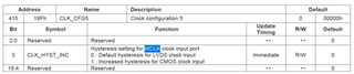
Here I set register 0x19D to 0x0040 and register 0x19F to 0x0008 for COMS to configure MCLK.

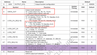
The LVDS output is configured with register 0x002 as 0x0400, register 0x0004 as 0x003, and register bit 0x00C3 as 0x195.
May I ask which registers need to be configured and what values are configured in order to comply with article 2 and 3?
