DAC60504: SPI write & read timing diagram with CRC polynomial

Part Number: DAC60504

Tool/software:

Hi team,

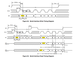
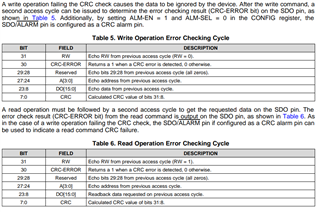
Customer is asking how the SPI write & read timing diagram with CRC polynomial work. So could you give examples of SPI write & read timing diagram with CRC polynomial? In case of write operation, could you also add the second access cycle to to determine the error checking result?

And according the datasheet as below, by setting ALM-EN = 1 and ALM-SEL = 0 in the CONFIG register, the SDO/ALARM pin is configured as a CRC alarm pin. Could you also give examples of how the CRC alrm pin work?

Regards,

Noriyuki Takahashi

  • Hi Takahashi-san, 

    The timing diagram is the same as shown in figure 62, but with 32 total bits instead of 24:

    The order of the data bytes is shown here:

    A write will fail if the CRC is incorrect. During the next read or write operation, the data shown in table 5 (or table 6 for a read) will be output on the SDO pin. Bit 30 will indicate if there was a CRC error in the last communication frame. 

    If the SDO/ALARM pin is configured as the CRC-ALARM, the pin will go low after the rising edge of CS when a CRC error is detected and returns high on the next successful SPI command (after CS rising edge, assuming no CRC error).

    Best,

    Katlynne Jones