This thread has been locked.

If you have a related question, please click the "Ask a related question" button in the top right corner. The newly created question will be automatically linked to this question.

DAC12DL3200: Biasing the outputs

Part Number: DAC12DL3200
Other Parts Discussed in Thread: TRF370417

Tool/software:

Hi,

As per the below mentioned forum we are using resistive bias circuit at the output of the DAC.

https://e2e.ti.com/support/data-converters-group/data-converters/f/data-converters-forum/1365129/dac12dl3200-biasing-the-outputs?tisearch=e2e-sitesearch&keymatch=DAC12DL3200# 

As per the calculations shared, we connected one pullup resistor and one pulldown resistor as below.

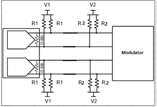
Voltage V1 is 1.8V and V2 is GND.

For getting a bias voltage of 1.55V and swing of 475mV with Full scale current of 19mA, value calculated for R1 is 50 Ohms & R2 is 3600 Ohms.

We mounted the same values, but when checking the DAC NCO output with different frequencies, the CM voltage and swing at the DAC output is varying.

For frequency of 100MHz: CM voltage is 1.2V and swing is ~390mV. because of this my dac output is going less than the compliance range. i.e., lower voltage is at ~1 V and compliance range is 1.3V.

For frequency of 200MHz: CM voltage changed to ~1.1V and swing got reduced to 200mV. In this case also my DAC output is going less than compliance range.

Why are swing and common mode voltage varying from frequency to frequency?

Also Vbias should be maintained at 1.55V as per the calculations?

Please correct if we are missing something.

Thanks in Advance. 

  • Hi Charan,

    Please let me know the Modulator that are you trying to interface to. Or please provide a schematic.

    Thanks,

    Rob

  • Hi Rob,

    We are using TRF370417 as our modulator. Please find the attached schematic.

  • Hi Charan,

    From the schematics posted, it does not look like the recommendation was followed that is clearly outlined in the TRF modulator datasheet. Page 22.

    See below. Following this procedure will bias the outputs of the DAC and inputs of the modulator correctly.

    I would also recommend starting out with the proper interface, but removing the filter and shorting this out for direct connection.

    Regards,

    Rob

  • Hi Rob,

    Thank you very much for the reply and suggestion. We will modify and check as per the suggestion.

    According to the datasheet, we can operate modulator with different common mode voltage other than 1.7V but OIP3 will not be optimal. We made a tradeoff with the common mode voltage as 1.55V common mode voltage will also meet our requirement. That is the reason we were not using the circuit mentioned in datasheet.

    Can you please clarify, how is swing and common mode voltage is getting varied for different frequencies?

    Also can you please provide any application note (other than :https://www.ti.com/lit/an/slaa399/slaa399.pdf?ts=1726724596446&ref_url=https%253A%252F%252Fwww.google.com%252F) that provides the calculation of these bias resistors? I would like to understand if I am missing any thing while calculating the resistor values.

    Thanks in Advance.

  • Hi Charan,

    Try optimizing the common mode voltages first with no filter in-between the two devices, change the freq and see if the CMV deviates. 

    Once you have achieved a stable CMV, then implement the filter.

    Right now the filter is probably coming into play on why the CMV is varying at different freqs....and you have no termination on the modulator side.

    Unfortunately, I don't know of any other app notes that help here with this specifically. However, this paper might help for implementing filters in-between active devices: www.ti.com/.../slyt853.pdf

    For the final lineup, I would implement your circuit this way:

    DAC - pullup resistor - series resistor - back term resistor in shunt - filter - back term resistor in shunt - series resistor - pulldown resistor - modulator

    The back termination resistor will have keep the impedance stiff on either side of the filter, as there will always be some mis-match...as I assume the traces are a bit long. The series resistor should be split in half and be on either side of the filter, this will also help.

    Regards,

    Rob

  • Hi Rob,

    Thank you very much for the reply. Will update after implementing.