This thread has been locked.

If you have a related question, please click the "Ask a related question" button in the top right corner. The newly created question will be automatically linked to this question.

DAC60504: Design for verification

Part Number: DAC60504

Tool/software:

Hello,

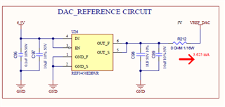
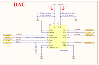
We are using DAC60504BRTET, in one of our design. As per our requirements we have designed the circuit. We have provided 5V to VDD and REF using 'REF3450IDBVR'. We interfaced DAC using SPI with controller 'PIC32MZ2048EFH144-I/PH'. We have provided 3.3V to VIO, SPI levels are 3.3V. As per our requirements, DAC output signal need to be max 5V. 

I have attached images of DAC60504BRTET and REF3450IDBVR' circuits can you please verify if the circuit design is functionally and electrically correct or not? Please let us know, if any changes are required.

  • Hi Nitesh,

    Pin 9 RSTSEL does not reset the device. When set to GND the DACs will start up at zero-scale, and when set to VIO the DACs will start up at midscale. I recommend tying this pin to either GND or VIO depending on what output behavior you want. 

    To reset the device, you can either do a power-on reset or a software reset.

    Also make sure you have enough current headroom to sustain the expected DAC loads. The DAC current is sourced from VDD. 

    Thanks,
    Erin

  • Hello Erin, 

    Thanks for the review and suggestions. We are connecting RSTSEL to GND.