This thread has been locked.

If you have a related question, please click the "Ask a related question" button in the top right corner. The newly created question will be automatically linked to this question.

ADS1288: ADS1288

Part Number: ADS1288
Other Parts Discussed in Thread: ADS1285, THS4551, ADS131E04, ADS131A04, ADS131M04, ADS1262, ADS1274, ADS127L14, THP210, ADS127L11

Tool/software:

Hello,

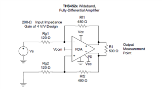
I am designing a circuit to interface single-ended sensor to ADS1288.

I would like to use internal PGA's fully differential amplifier, but I need to match output impedance of the sensor (actual value is 32kOhm) to input impedance of the differential amplifer.    

Please tell me an idea how to simulate input circuitry of the PGA?

Thank you very much.

  • Hi Lkhagvajantsan,

    Good to meet you on the TI e2e forum.

    The PGA of the ADS1288 is an instrumentation amplifier with very high input impedance (500Mohm) as determined by the first derivative of the input current vs input voltage curve.

    Unfortunately, a Spice model for ADC is not available.

    One solution is to ground the negative ADC input and drive the signal on the positive input, using an impedance matching 32kohm resistor connected to ground (+/-2.5V power supplies). One concern is the single ended signal creates an effective common mode signal component between the two inputs that could lead to degradation of THD performance. The THD effect is given by the ADC's ability to reject common signals (CMRR). I suggest evaluating ADC performance when using single ended signals using the ADC eval board. Unfortunately, the ADS1288 eval board is not available, but ADS1285 eval boards are available, which is the same type ADC architecture, and can serve as a valid proxy. https://www.ti.com/tool/ADS1285EVM-PDK

    Regards,

    Mark

  • Hello Mark,

    Thank you vey much for your reply.

    The sensor what I am talking about is MEMS Accelerometer model ADXL354, the application is seismic monitoring.

    I already requested Alec to support designing THS4551 based front end.

    Now we need to select proper ADC. The data sheet of the ADXL354 gives sensitivity as 400 mV/g typical, and its output noise density as 22 μg/√Hz. So for a 100 Hz bandwidth, this translates to an output voltage noise level of
    En = 0.4 V/g * 22 μg/√Hz * √100Hz = 88 μV rms. Based on this I calculate DR=20*Log(MAX SIGNAL/NOISE)=76dB.

    Could you please suggest 24bit low noise, low sampling rate, 4 channel simultaneous sampling Delta Sigma ADC, suitable for seismic application.

    Thank you and best regards,

    Lhagva 

  • Hi Lkhagvajantsan,

    The 4-channel electrical grid ADCs could all be good fits for your application. They are designed for the low frequency range.

    https://www.ti.com/product/ADS131E04

    https://www.ti.com/product/ADS131A04

    https://www.ti.com/product/ADS131M04

    These ADCs (E, A or M ADC family) perform similarly with differences in sample rates, input range/impedance and power supply options

    Regards,

    Mark

  • Hi Mark,

    Thank you very much for suggesting the ADC ADS131X04.

    From the datasheet, I see that this ADC supports simultaneous sampling of 4 channels.

    My application involves a 3-channel MEMS accelerometer for seismic signal acquisition. Do you think simultaneous sampling would still be possible with the internal multiplexer, or would I need a separate ADC for each channel?

    Additionally, could you clarify the minimum allowable value for the master clock frequency?

    Best regards,

    Lhagva

  • Hi Lkhagvajantsan,

    I recommend a simultaneous-sampling ADC for ac applications, in which one ADC is used for each channel such as provided by the ADS123X04 family, rather than multiplexing a single ADC. Multiplexed data acquisition for ac applications requires post processing the data to correct the time shift between channels and despite the time shift correction, the end result of the data is not as good as simultaneous sampling data. Most seismic data acquisition use simultaneous sampling ADCs for the three axis data.

    Multiplexing a single ADC is fine for DC measurements, such as weight, temperature inputs and DC V/I test applications.

    Min clock frequencies

    ADS131E04: 1MHz

    ADS131A04: 0.2Mhz

    ADS131M04: 0.3MHz

    All the ADS131x04 ADCs provide programmable OSR to adjust the data rate, signal bandwidth and noise to suit your requirements. Exact data rates are achieved by selecting the next lower OSR value (next higher data rate) then slowing the clock frequency as appropriate.

    Regards,

    Mark

  • Hi Mark,

    We have purchased ADS1285 kit and starting test and evaluation of geophone signals.

    What is your opinion about ADS1262 32bit ADC for seismic application (0.1Hz to 100Hz signals).

    Since ADS1262 is not simultaneous sampling, is there any effect of multiplexing for seismic signals.

    Best regards,

    Lhagva 

  • Hi Lkhagvajantsan,

    The ADS1285 has been specifically designed to interface with geophone sensors while consuming very small 5mW while providing very high dynamic range. It is a good choice for seismic data acquisition.

    The main issue of the ADS1262 for seismic data acquisition is signal aliasing. The signal is aliased by two mechanisms:

    1) The ADS1262 sinc filter provides very little rejection at the Nyquist frequency and above (> fs/2). This type of filter is not optimal for ac applications because of the aliasing.

    2) Even if the ADS1262 had an optimal brickwall filter (such as in the ADS1285), multiplexing causes further aliasing problems because the effective sample rate due to multiplexing is now shifted to within passband of the filter, so there is no aliasing protection at fs/2.

    I recommend ADS1285 or lower cost ADS1288 for seismic data acquisition.

    Regards,

    Mark

  • Hello Mark,

    I have been looking at datasheets of ADS131X04 series.

    I think ADS131E04 or ADS131A04 is suitable for MEMS accelerometer and set sampling rate to about 100 SPS. 

    However datasheet does not show noise measurements results at lower SPS.

    Could you please give me example circuit which used external oscillator for clock input.

    What do you think about ADS1274 for this application? Also the datasheet of ADS1274 does not show noise measurement for low SPS.

    Best regards,

    Lhagva

  • Hi Lkhagvajantsan,

    As you noted, the ADS131E04, ADS131A04 do not provide 100SPS sample rate. Usually on many ADCs, you can slow the master clock by 10x at 1kSPS to yield 100SPS, but the ADS131x devices do not allow such a low clock frequency. Incidentally, the noise at 100SPS is the same as 1kSPS when slowing the clock frequency. A better approach is to implement an external decimating filter. That is, accumulate and average ten readings from the ADC at 1kSPS so the averaged output rate is 1/10 the input rate. The noise of the input data to the filter will reduce when averaging by sqrt(N), where N is the averaging number. Incidentally, if possible average data with N=8 (125Hz output rate), so to divide the running sum by 8 involves three bit shifts to the right, no division math needed.

    A one-chip clock oscillator such as from ECS will work fine. Apply the clock signal to the ADC CLK pin. https://ecsxtal.com/store/pdf/ECS-2520MVLC.pdf

    The latest generation ADS127L14 is an improved device over the ADS1274. It will release in 1-2 weeks. https://www.ti.com/lit/ds/symlink/ads127l14.pdf

    The ADS127L14 has much better noise performance vs ADS131x, with one channel powered down for three channel applications. It also has four speed modes and many OSR settings available to change the data rate and to satisfy noise requirement. 102.4 SPS is the closest using max speed mode and the sinc3+sinc1 filter. To yield exactly 100SPS, slow the master clock accordingly for precise 100SPS.

    Regards,

    Mark

  • Hello Mark,

    Thank you for your reply.

    Yes, ADS127L14 has better noise performance.

    What do you mean one channel powered down for three channel applications.

    Please let me know when the product is released.

    Best regards,

    Lhagva

  • Hi Lkhagvajantsan,

    One channel of the ADS127L14 can be powered-off to save power, leaving three active channels.

    ADS127L14 release is approximately 2 weeks out. Parts are in inventory, and now waiting for completion of the release paper work.

    -Mark

  • Hello Mark,

    Thank you for your reply. I think we will use ADS127L14 for MEMS accelerometer.

    Coming back to talk of geophone and ADS1285/1288 we needed to use THP210 to drive ADC.

    I have two questions.

    1. When I use Vref = 4.096V, what will be highest differential voltages at the input of ADC without distorting.

    2. Can we connect Vocm of the THP210 to ground.

    Please see below schematics and transient analysis results, is it correct topology?

    Best regards,

    Lhagva

  • Hi Lagva,

    That's great. The ADS127L14 was released today. It should appear live on TI.com tomorrow.

    The ADS127L14 has two programmable input ranges: +/-Vref and +/-2Vref. For the +/-Vref range, Vref = 4.096V is fine. You can use the 2x input range with Vref = 4.096V, but the full dynamic input range is limited by the 5V power supply, so Vref=2.5V is a better choice for 2x input range. But I would stick with1x input range and Vref=4.096V

    With the ADC operated by +/-2.5V supplies, grounding the THP210 Vocm pin is fine. 

    The voltages waveforms also  look fine.

    For the THP210 stage, you may want use feedback caps from the output to input to help stability. I think the circuit appears stable, but it is worth checking to be sure. 

    https://www.ti.com/video/4080346918001?keyMatch=op%20amp%20stability&tisearch=universal_search

    This video at the 8:20 mark shows how to use the TI TINA spice program of THP210 spice model to test stability by inserting super-large inductor and capacitor into your actual circuit then analyzing the phase response at the THP210 output pins. The other method is to stimulate with a square wave input. If the THP210 output only has 10%  peaking, then the circuit stable.

    https://www.ti.com/lit/pdf/sboa546

    Above is a THP210 + ADS127L11 application note.

    Is the 1st stage a combination HPF and LPF within the inner loop op-amp? I will have to look at this circuit a little more to fully grasp it.

    Regards,

    Mark

  • Hello Mark,

    Conguratulations! Nice to hear that TI releasing the ADS127L14.

    I think this ADC is perfect match for our application.

    But I would stick with1x input range and Vref=4.096V

    I understand that you prefer to use 1x input range and Vref=4.096V. 

    So the power supply will be +5V and -5V, Vocm pin of the THP210 is grounded, am I right?

    As for the THP210 stage, I will read document thoroughly and take care of that.

    As for 1st stage, the natural frequency of geophone (attached is equivalent circuit and frequency response of geophone) is 4.5Hz and it limits their measurable low-frequency range, we are trying to extend lower frequency response down to 0.5Hz. U1 is LPF and U2 is subtraction circuit. 

    There is a paper describes it in detail, let me attach here.

    Best regards,

    Lhagva

    An Effective Method for Improving Low-Frequency Response of Geophone.pdf

  • Hi Lagva,

    One clarification, the THP210 should be operated with +/-2.5V supplies, same supplies used for the ADC. The GND pin of the 4.096V reference and ADC REFN pin connects to -2.5V. Route the trace of the ADC REFN pin to the GND pin of the reference, then connect to -2.5V. This avoids picking up noise and signal induced currents from the -2.5V supply.

    Thank you for the paper, it is interesting. I will take time to read it and supply comments if warranted.

    Regards,

    Mark