Tool/software:
Dear Mr/Mrs
Problem: reading back a value from DAC8574
We use several DAC8574 on a PCB
We use multiple DAC8574 on a bus as stated in the datasheet: "Address Support for up to Sixteen DAC8574s"
We use addresses lines on the chips A3, A2, A1 and A0
AA-AA
10 32
U10: Adres 1001100-01
U12: Adres 1001101-01
U16: Adres 1001110-01
U18: Adres 1001111-01
U11: Adres 1001100-10
U13: Adres 1001101-10
U15: Adres 1001110-10
U17: Adres 1001111-10
I am testing with 1 of the chips to readback a value?
When I write a value to the chip in this case 0x11 I read back 0.
I know it muist be reading something because the uPWD byte is showing 0x3F
The numbers are hex
Test Program gives me
Write DAC8574 Oke
Address: 98 50 Data 0 11
Read DAC8574 Oke
Address: 98 51 Data [3F] 0 0
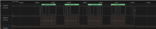
The write sequence
ACK ACK
slave Master
I2C_Start mACKs
Write Adress 0x98 sACK 10011000
Write Control 0x50 sACK 01010000
Write MSB 0x00 sACK 00000000
Write LSB 0x11 sACK 00010001
I2C_Stop
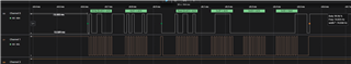
The read sequence
ACK ACK
slave Master
I2C_Start mACKs
Write Adress 0x98 sACK 10011000
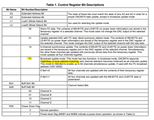
Write Control 0x51 sACK PD0=1 01010001
Restart
Write Adress+1 0x99 sACK
Read uPWD mACK 00111111
Read MSB mACK 00000000
Read LSB mNACK 00000000
I2C_Stop
sACK = Slave ACK
mACK - Master ACK
mNACk = Master no Ack
fprintf(MASTER_DEBUG_STREAM, "Write DAC8574 Oke\r\n");
fprintf(MASTER_DEBUG_STREAM, "Address: %X %X Data %X %X \r\n", ADDRReg, CTRLReg, MSB, LSB );
fprintf(MASTER_DEBUG_STREAM, "Read DAC8574 Oke\r\n");
fprintf(MASTER_DEBUG_STREAM, "Address: %X %X Data [%X] %X %X\r\n", ADDRReg, CTRLReg, uPWD, MSB, LSB );