This thread has been locked.

If you have a related question, please click the "Ask a related question" button in the top right corner. The newly created question will be automatically linked to this question.

DAC60501: Power up not going to zero volts

Part Number: DAC60501
Other Parts Discussed in Thread: OPA192,

Tool/software:

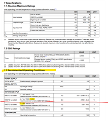
We have a new PCB we've spun that incorporates that DAC60501ZDGS, which according to the data sheet, should power up at zero V out.


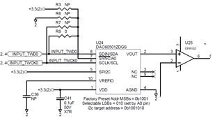
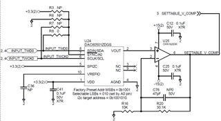
As you can see, we're trying to run the DAC off 3.3V. In addition, you'll see we're trying to run it in i2c mode. For the i2c address, we desire 0x02 (010), so we've tied A0 to the i2c data line.

Before I've even tried to write/read to the command registers, upon powerup, I'm observing Vout is around +830mV. More concerning, I'm observing VREFIO reading about 3.23V. If I understand the data sheet and the power on state of the chip, VREFIO should be an output and I should be seeing the internal 2.5V signal present.

Thinking we were doing something odd, we whitewired the 3.3(2) rail to be 5(2) on a second board. Upon doing this, the VREFIO measured 2.5V dead on, which was nice to see. However, Vout was measuring not zero, at +908mV.

The 3.3V measurements were made on one PCB, and the 5V config was done on a second. So I have 2 boards with DAC60501s that are exhibiting this problem. In addition, I lifted the pin on the OPA192 on the 5V config, to ensure the DAC60501 was unloaded, and it still exhibited this behavior.

The part markings on the chip are as follows:

TI27
P30RA
651Z

I attempted to communicate via i2c, and this appears to be working. I can write registers and read them back. I know I'm truly talking to the chip, due to the ACKs I'm seeing on the i2c bus, plus when I read the DEVID register, the non reserved RESOLUTION and RSTSEL bits are set appropriately. I can also write to the DAC CODE register and read the value back. However, Vout stays at the above mentioned voltages. Post power up, I've tried issuing a SOFT RESET via the TRIGGER register to no avail. I've also experimented with changing the DAC SYNC EN bit and writing the LDAC bit after writing a new DAC CODE, all to no avail.

My 5V and 3.3V rails seem to come up in about 1mS.

I'm at a bit of a loss here and would appreciate any insights as to what might be going on with this chip. I don't see what my Vout should be anything but zero. The only response I seem to be getting from the chip with my i2c commands is when I set the REF_PWDWN bit in CONFIG, I see the VREFIO line go to zero. However when I set the DAC_PWDWN bit to 1, the output still 'stays stuck' and the voltages I mentioned above.


Thank you for your help.

  • Hi Adam, 

    I do agree with you that seeing 3.3V on VREFIO is the point of concern. Are you seeing this behavior across multiple boards/devices? What are your I2C lines pulled up to? 

    It seems like there is some issue with the analog portions of the device (reference and output circuitry). 

    Best,

    Katlynne Jones

  • Hello Katlynne, thank you for the quick replay.

    I've only tried this on two boards so far, so I have a few more to try.

    The i2c lines are pulled up to +3.3(2) with fairly strong pull ups, on the order of 2kOhm. Again, it appears I'm communicating properly with the device, when I look at the lines with a logic analyzer.

    I'm to the point where I've stopped sending i2c commands from my micro upon power up of the board, just trying to assess to the power on state of the DAC60501. 

    A few things just to clarify, when it comes to assessing power on state:
    1) I take the the registers on the chip are non volatile? So when I power cycle, I should see the reset values called on in the data sheet? Just wanted to make sure, that as i'm experimenting writing and reading from the registers, I should always be guaranteed a clean state upon power cycle.

    2)Generally speaking, the configuration of VDD = +3.3V looks like its valid according to the data sheet. However, it does look like I need to setup the gain and DIV registers appropriately if I want to get full scale output, else the alarm bit will set. I guess what I'm getting at is, am I potentially setting myself up for risk of damanging the chip by trying to use a 3.3V VDD config (naturlaly assuming I have clean power rails that don't have over voltage transients, etc), or is 5V VDD the recommended best practice for the chip, knowing the default state of the internal ref and gain and DIV regsiters?

  • Sorry, I forgot to ask, what would you expect to see on VREFIO and VOUT output pin upon power up (before my micro tires to initialize the chip and write any registers), based on the +3.3V VDD configuration I have shown in the schematic above, and knowing the default state of the chip?

  • Hi Adam,

    1) Yes, you should see the reset values after every power cycle. As long as you are fully power cycling the DAC (VDD down to 0V and back up to 3.3V), you should have a clean state on power cycle. Brown out conditions aren't guaranteed a clean slate because it is unknown if the DAC actually went through the POR process. Some registers might have reset and others might not have, or been corrupted.

    How fast after startup are you writing any new values to the DAC?

    2) There would be no damage to the chip if the gain and div registers were set incorrectly. The output buffer will just shut down and you won't see any output on VOUT. That shouldn't be an issue as long as you eventually configure the correct values after startup. 

    3)  With the default configuration and a 3.3V VDD, you should see 2.5V on VREFIO and 0V on VOUT. The VREFIO pin sees the reference voltage before the divider, so the divider setting wouldn't affect what you're seeing there. 

    Best,

    Katlynne Jones

  • Thank you for your reply.

    It's at least 100mS after Vcc stabilizes at 3.3V, the host micro starts talking to the DAC.

    I've experimented with a few different boards, and my issues seemed to be isolated to one or two boards. However, I just experienced a scenario where I was developing code most of the afternoon on the board, and the DAC was responding properly. I then loaded in a new version of FW for an additional test, and I started observing Vout 'stuck' at 2.91V On the surface, it appeared my firmware 'broke the DAC', which seems incredibly unlikely, which is what led to the earlier question regarding improper configurations and potentially damaging the chip. I had a second board which also had similar behavior, except its power on Vout was 3.23V. I can replace the DAC, and the circuit starts behaving again...

    My first instinct was to stick a scope of the rails and various pins, just to see if I could see any unexpected transients as I power cycle the board. I have not seen any unexpected transients to this point.

    I guess what I'm asking is

    a) are there any known issues in the chip or specific pins,  that I need to be 'extra' careful in ensuring no transients occur?
    b) based on the schematic design presented, just from an initial glance, does TI see anything that may be risky with my 3.3V configuration? The reason for that question relates to an observation in the datasheet. Granted, it's regarding the use case where a user would feed the chip a reference input voltage. But I couldn't help but notice a clear distinction of the VREFIO min/max (when I assumed configured as an input), if Vcc is 3.3V. I'm curious if there's some kind of internal threshold where I'm right on the edge 'of something', powering the chip from 3.3V? And if so, would it make more sense to power the chip from 5V, for better reliability?


    Again, our schematic:


    Any suggestions would be welcome to help mitigate any damage to the chip that would cause Vout to get 'stuck' at some output voltage.

  • Hi Adam, 

    A) Not as far as I know, and I'm not seeing anything documented internally. All pins have the same input protection (ESD diode to VDD/ground). 

    B) I don't see anything risky with the schematic. Improper configuration of the VREFIO pin according to the recommended operating conditions table would not damage the device. it just won't operate properly. Operating VREFIO outside of the absolute maximum ratings table would damage the device. You're using the internal reference, so there is no risk of improper VREFIO/VDD power sequencing. You could power the chip with 5V to be outside of that edge condition, but I'm not so sure this is the source of your issue, so I wouldn't be able to say if this would help. 

    Is replacing the DAC the only way to get out of the stuck condition? Power cycling or software resets don't help? Since replacing the DAC on the 2.91V stuck DAC, have any DACs on that board seen issues with the new FW? 

    Best,

    Katlynne Jones