Other Parts Discussed in Thread: ADS9813
Tool/software:
Hello,
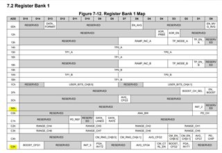
We are using the ADS9813 EVM along with the Zynq 7045 FPGA. The ADS9813 is mounted on the FMC of the FPGA. We plan to use the ADS9813 in a 4-lane SDR data rate configuration.
We have built and verified the logic for this setup in Vivado through simulation, and now we intend to implement it on hardware. However, we encountered some confusion regarding the initialization sequence in the ADS9813 datasheet. Our queries are as follows:
- In Table 6-13 (Initialization Sequence), register 0x04 is mentioned with a value of 0x000B, but on page 39, it is stated to write 0x0003. Could you clarify the correct value?
- Registers 0x92 and 0xC5 belong to Bank 1, but Table 6-13 mentions selecting Bank 2 for these registers. Is this a mistake, or is there a specific reason for this?
- While observing fCLK in the ILA with the dCLK as the clock, we notice that fCLK is sometimes missing and does not appear as expected. Could you explain why this might be happening and provide suggestions to resolve it?
Also if Iam configuring sdr mode then fclk rise edge to rise edge there should be 48 dclks . even if spi write is not done then for default configuration i.e ddr data rate with 4 data lanes it should be 24 dclks but iam not seeing fclk is repetiting for these dclks. it is repetitting for 65 dclks and 130 dclks sometimes and also missig for certain number of dclks. - when we try initialize the registers 0x92 and 0XC5 by selecting bank 1 we are experiencing a power down situation where all data lanes and fclk are logic low.
It would be helpful if you could provide the correct final initialization sequence for the ADS9813 and clarify the behavior of fCLK.
Best regards