ADC12DJ3200: Unable to get the output in JMODE-10 configuration

Part Number: ADC12DJ3200

Tool/software:

Hi,

I configured the ADC12DJ3200 to JMODE-6 (8-bit, 4-lanes, dual channel) by setting the following parameters -


             Sampling Frequency = 1600 MHz
             ADC input clock         = 1600 MHz
             line rate                     = 8 Gsps
            JESD ref_clock          = 200 MHz
            SYSREF Frequency  = 5 MHz

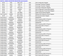
Later, I configured the ADC registers as follows -
-------------------------------------------------------
ADDRESS   |   DATA
-------------------------------------------------------
//////// ADC Registers

0x0000            0x30
0x0002            0x00
0x0003            0x03
0x0004            0x20
0x0005            0x00
0x0006            0x05
0x000C           0x51
0x000D           0x04
0x0010            0x00
0x0029            0x20
0x0029            0x60
0x002A            0x00
0x002C            0x00
0x002D            0x00
0x002E            0x00
0x0030            0xC4
0x0031            0xA4
0x0032            0xC4
0x0033            0xA4
0x0038            0x00
0x003B            0x00
0x0048            0x00
0x0060            0x00
0x0061            0x01
0x0062            0x01
0x006A            0x00
0x006B           0x00
0x006C           0x01
0x0070           0x01
0x0071           0x00
0x007A           0x00
0x007B           0x00
0x007C           0x00
0x007E           0x00
0x007F           0x00
0x0080           0x00
0x0081           0x00
0x0082           0x00
0x0083           0x00
0x0084           0x00
0x0085           0x00
0x0086           0x00
0x0087           0x00
0x0088           0x00
0x0089           0x00
0x008A           0x00
0x008B          0x00
0x008C          0x00
0x008D          0x00
0x008E          0x00
0x008F          0x00
0x0090          0x00
0x0091          0x00
0x0092          0x00
0x0093          0x00
0x0094          0x00
0x0095          0x00
0x0102          0x00
0x0103          0x00
0x0112          0x00
0x0113          0x00
0x0122          0x00
0x0123          0x00
0x0132          0x00
0x0133          0x00
0x0142          0x00
0x0143          0x00
0x0152          0x00
0x0153          0x00
0x0160          0x00
0x0200          0x00
0x0061          0x00
0x0201          0x06
0x0202          0x1F
0x0203          0x01
0x0204          0x02
0x0205          0x00
0x0206          0x00
0x0207          0x00
0x0208          0x00
0x0209          0x00
0x0061          0x01
0x0000          100
0x0200           0x01
0x0210           0x00
0x0211           0xF2
0x0212           0xAB
0x0213           0x07
0x0214           0x01
0x0215           0x00
0x0216           0x02
0x0217           0x00
0x0218           0x00
0x0219           0x02
0x0297           0x00
0x02B0          0x00
0x02B1          0x05
0x02B2          0x00
0x02B3          0x00
0x02B4          0x00
0x02B5          0x00
0x02B6          0x00
0x02B7          0x00
0x02C0          0x00
0x02C1          0x1F
0x02C2          0x00

With these registers I am able to observe the sine wave generated from the ADC samples.

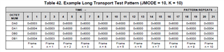
Now, I am trying to configure the ADC12DJ3200 in JMODE-10 (15-bit, 4-lanes, decimate by 4) with the following settings -


         Sampling Frequency  = 1600 MHz
         ADC input clock         = 1600 MHz
         line rate                     = 8 Gsps
         JESD ref_clk             = 200 MHz
         SYSREF Frequency  = 12.5 MHz

The ADC  registers are configured as follows -
----------------------------------------------
ADDRESS   |    DATA
----------------------------------------------
/////// ADC Registers

0x0000            0x30
0x0002            0x00
0x0003            0x03
0x0004            0x20
0x0005            0x00
0x0006            0x05
0x000C           0x51
0x000D           0x04
0x0010            0x00
0x0029            0x20
0x0029            0x60
0x002A            0x00
0x002C            0x00
0x002D            0x00
0x002E            0x00
0x0030            0xC4
0x0031            0xA4
0x0032            0xC4
0x0033            0xA4
0x0038            0x00
0x003B            0x00
0x0048            0x00
0x0060            0x00
0x0061            0x01
0x0062            0x01
0x006A            0x00
0x006B           0x00
0x006C           0x01
0x0070           0x01
0x0071           0x00
0x007A           0x00
0x007B           0x00
0x007C           0x00
0x007E           0x00
0x007F           0x00
0x0080           0x00
0x0081           0x00
0x0082           0x00
0x0083           0x00
0x0084           0x00
0x0085           0x00
0x0086           0x00
0x0087           0x00
0x0088           0x00
0x0089           0x00
0x008A           0x00
0x008B          0x00
0x008C          0x00
0x008D          0x00
0x008E          0x00
0x008F          0x00
0x0090          0x00
0x0091          0x00
0x0092          0x00
0x0093          0x00
0x0094          0x00
0x0095          0x00
0x0102          0x00
0x0103          0x00
0x0112          0x00
0x0113          0x00
0x0122          0x00
0x0123          0x00
0x0132          0x00
0x0133          0x00
0x0142          0x00
0x0143          0x00
0x0152          0x00
0x0153          0x00
0x0160          0x00
0x0200          0x00
0x0061          0x00
0x0201          0x0A
0x0202          0x1F
0x0203          0x01
0x0204          0x02
0x0205          0x00
0x0206          0x00
0x0207          0x00
0x0208          0x00
0x0209          0x00
0x0061          0x01
0x0000          100
0x0200           0x01
0x0210           0x00
0x0211           0xF2
0x0212           0xAB
0x0213           0x07
0x0214           0x01
0x0215           0x00
0x0216           0x02
0x0217           0x00
0x0218           0x00
0x0219           0x02
0x0297           0x00
0x02B0          0x00
0x02B1          0x05
0x02B2          0x00
0x02B3          0x00
0x02B4          0x00
0x02B5          0x00
0x02B6          0x00
0x02B7          0x00
0x02C0          0x00
0x02C1          0x1F
0x02C2          0x00


Except the above two registers remaining are left unchanged.
I am able to get the DATA_VALID, SYNC and SYSREF signals as expected. But I am unable to generate the sine wave output from the ADC samples.


I have the following queries regarding this -

1. As the JMODE-10 configuration involves decimate by 4 setting, do I need to change any NCO registers for that ? If so, request you to help me in setting that parameter.

2. I also rearranged the mapper that takes samples as per JMODE-10 but as I am getting a distorted signal, are there any other settings that need to be considered ?

Regards,

Anirudh 

  • Hi Anirudh,

    With any JMODE, assuming the JESD link comes up without errors, the recommendation is to first put the ADC in transport layer test pattern mode. This puts out a defined pattern from the ADC, which will help test the lane/sample mapper in the FPGA. If that works, you can then move on to testing the full ADC path. 


    With decimation enabled, if the NCO is set to 0, the input tone will essentially pass through to the I (assuming it’s at a low enough frequency where it doesn’t get filtered out by the decimation filter). Alternatively, you can feed an input tone of NCO+x and see the output post mixing and filtering. 

    Regards,

    Ameet 

  • Hello ,

    I've configured JMode 10 with a long test pattern by writing to the register at address 0x205 with data 0x05. However, the resulting frame appears different from what is shown in the datasheet. Is this behavior justified?

    datasheet  test pattern is as attached

    request you help us resolve the issue. 

  • Hi Anirudh,

    The ILA capture shows the lane data from the JESD IP. Kindly map the lane data to samples, as that will enable us to determine if the values are as defined in the table for the long test pattern. 

    Regards,

    Ameet

  • Hi Ameet,

    The below figure shows the 16-bit sample data of JMODE-10 when ran in long transport test pattern.

    I also tested the configuration for ramp mode and it is generated as expected.

    We would like to inform you that our custom board is functioning perfectly with JMODE 6, and we are successfully capturing data while achieving the required performance.

    However, we are encountering an issue with JMODE 10. As mentioned earlier, we are getting the SYNC and VALID signals high, but we are not seeing any change in the JESD output data(rx_data) when we feed data from the source( i couldnt see any transistion in bits when we feed input from signal generator in rx_data of jesd ip).

    we feel we are missing some register to enable NCO.

    Could you please help us identify what might be missing or provide suggestions on how to resolve this issue?

  • Hello Anirudh,

    Please use the following registers to configure the NCO 

    and you can also use equation (4) on pg 50 to calculate the frequency word to program to the adc.

    Best,

    Eric

  • Hi Eric,

    I am writing the following registers to configure the NCO for JMODE-10:

    Address     Data


    0x0000       0x30
    0x0002       0x00
    0x0003       0x03
    0x0004       0x20
    0x0005       0x00
    0x0006       0x05
    0x000C       0x51
    0x000D       0x04
    0x0010        0x00
    0x0029        0x20
    0x0029        0x60
    0x002A        0x00
    0x002C       0x00
    0x002D       0x00
    0x002E        0x00
    0x0030        0xA0
    0x0031        0x00
    0x0032        0xC4
    0x0033        0xA4
    0x0038        0x00
    0x003B       0x00
    0x0048        0x00
    0x0060        0x00
    0x0200        0x00
    0x0061        0x00
    0x0201        0x0E
    0x0202        0x09
    0x0203        0x01
    0x0204        0x02
    0x0205        0x04
    0x0206        0x00
    0x0207        0x00
    0x0208        0x00
    0x0209        0x00
    0x0210        0x00
    0x0211        0xF2
    0x0212        0xAB
    0x0213        0x07
    0x0214        0x00
    0x0215        0x05
    0x0216        0x02
    0x0217        0x00
    0x0218        0x00
    0x0219        0x02
    0x0220        0x00
    0x0221        0x00
    0x0222       0x00
    0x0223       0x00
    0x0224       0x00
    0x0225       0x00
    0x0240       0x00
    0x0241       0x00
    0x0242       0x00
    0x0243       0x00
    0x0244       0x00
    0x0245       0x00
    0x0061       0x01
    0x0000       100
    0x0200       0x01
    0x006C      0x00
    0x0000       100
    0x006C       0x01
    0x0297       0x00
    0x02C0      0x00
    0x02C1       0x1F
    0x02C2      0x00

    But still I am not getting the output for the JMODE-10 configuration

  • Hello Anirudh,

    So you are configuring the NCO frequencies to zero? What is the tone you are inputting to the device?

    Thanks,

    Eric

  • Hi Eric,

    Yes, we are configuring the NCO frequencies to zero and the input tone to the device is 400MHz.

    Regards,

    Anirudh

  • Hello Anirudh,

    If your Fs is 1.6GHz and you are decimating by 4 then your bw will be +-400MHz so you will not be able to see a 400 MHz tone it will fall on the nyquist zone. Can you try decreasing the frequency or setting the nco to a higher frequency not zero.

    Thanks,

    Eric