


Part Number: DAC38J84EVM
Other Parts Discussed in Thread: DAC38J84, , LMK04828
Tool/software:
Hi ,
We are trying to ensure deterministic latency in Subclass1 mode between JESD204B TX IP using Efinix Titanium FPGA (Ti375N1156) and DAC38J84 EVM. LMK04828 on DAC38J84EVM is used to generate the required clocks and Sysref TO DAC as well as FPGA. Following is the configuration:
LMF = 442, K = 32, Interpolation = x4
Data Rate = 5 Gbps, FPGA_clk = 125 MHz, DAC_clk = 250 MHz, Sysref = 3.90625 MHz.
RBD = 15
Below is the reference setup Diagram used to achieve deterministic latency using the above setup.
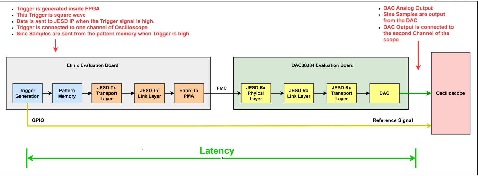
- Trigger pulse is generated at regular intervals , which is provided to two paths, one goes into Pattern Memory which starts sending samples to JESD204B TX IP on every rising edge of trigger pulse, and stops sending as soon as pulse goes low. Second path leads to DAC38J84EVM header through which it can be probed on oscilloscope along with DAC output.
- After every power cycle, Linkup sequence between JESD204C TX IP on FPGA Eval board and JESD204B Rx IP on DAC38J84 EVM is run. Once linkup is established (JESD204B reaches Data Phase) , Trigger pulse is started with fixed width and gap between the pulses. DAC output and trigger is probed on the Oscilloscope using SMA Cables.
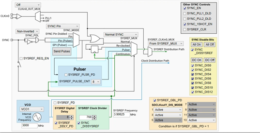
- LMK04828 generates Sysref in Pulsed Mode and all the Clock and Sysref Dividers are reset using Sync toggling. Below is the GUI snapshot of used configuration.
- Below attached figures gives a glimpse of the Oscilloscope Display. The green waveform represent rising edge of trigger pulse and the pink waveform represent DAC analog output with a delay of around 770ns delay between them.
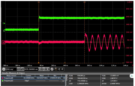
- 20 Iterations of power cycles and linkup sequences combined were executed to check deterministic latency. The value between the trigger rising edge and the output waveform had a uncertainty of 1.6 ns around the typical value of 770.738 ns (max = 771.22 ns, Min = 769.62 ns).
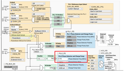
Also, we are using the Phase detector Frequency of 160 kHz in the PLL we are using as shown below.
So, we would light to get insight on the following points:
1) Why is there a 1.6 ns delay around the typical value ?
2) Is the low value of Phase Detector frequency responsible for the jitter in the resulting clocks, resulting in this variation ?
2) What can be done to minimise the value as much as possible ?
