Part Number: ADS131E08
Tool/software:
I'm reviving an old post I made a few months ago that I lost track of.
We have a design where we'd like to utilize the full, 24-bit range of the ADS131E08 ADC. We expected the full range to be +/-2^23 bits = +/-8,388,608.
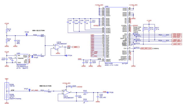
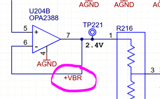
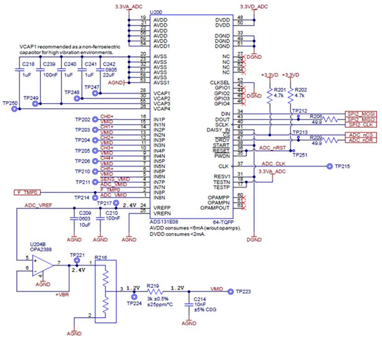
The positive input voltage range we use is 0 ~ 2.4V, and we have a fixed negative voltage of 1.2V for each channel. This way the differential input voltage range is +/-1.2V, and by using an internal ADC gain = 2 we achieve a differential input voltage range of approximately +/-2.4V.
Put simply, our issue is that we see ADC values getting stuck before we reach the bounds of the differential input. When we force the inputs to saturation by applying 2.4V or 0V at the positive input channel, the ADC output does not reach +/-8M.
We have seen this behavior on two designs. In the first, we supply the ADC with 3.3AVDD and connect AVSS to 0V GND. On the second AVDD is connected to 3.0V instead of 3.3V. In the first case we do see +8388607 on the positive end but we never reach -8388608 on the negative end. In the second case we do not reach 8M on the negative or positive ends.
Could I get some help understanding why this is happening and what we can do to utilize the full 24-bit range with our use case?
To answer the questions posed by Dale Li in the original post...
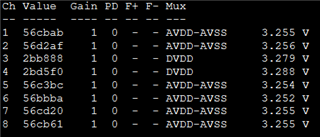
1. I'm not sure what you're referring to by calibration or offset error. In case 1, the saturation values are fairly consistent across multiple boards/chips. At PGA = 1, we only reach about -4M counts when applying 0V at the positive input.
| Case 1 | |||||
| Gain | 1 | 2 | 4 | 8 | 12 |
| Negative Codes | -4182489 | -5576058 | -6685939 | -7445348 | -7717432 |
| Positive Codes | 8388607 | 8388607 | 8388607 | 8388607 | 8388607 |
2. For case 2 -- yes, the 3.0V source is the only significant difference in this portion of the design.
| Case 2 | |||||
| Gain | 1 | 2 | 4 | 8 | 12 |
| Negative Codes | -4182489 | -5576058 | -6685939 | -7445348 | -7717432 |
| Positive Codes | 6272517 | 8373916 | 8388607 | 8388607 | 8388607 |