This thread has been locked.

If you have a related question, please click the "Ask a related question" button in the top right corner. The newly created question will be automatically linked to this question.

AFE881H1: UART COMMUNICATION PROBLEM

Part Number: AFE881H1
Other Parts Discussed in Thread: TLVH431, TLV431B

Tool/software:

Hello,

I am using AFE881h1 for HART Communication.

I wanted to use UBM mode but I have a problem.

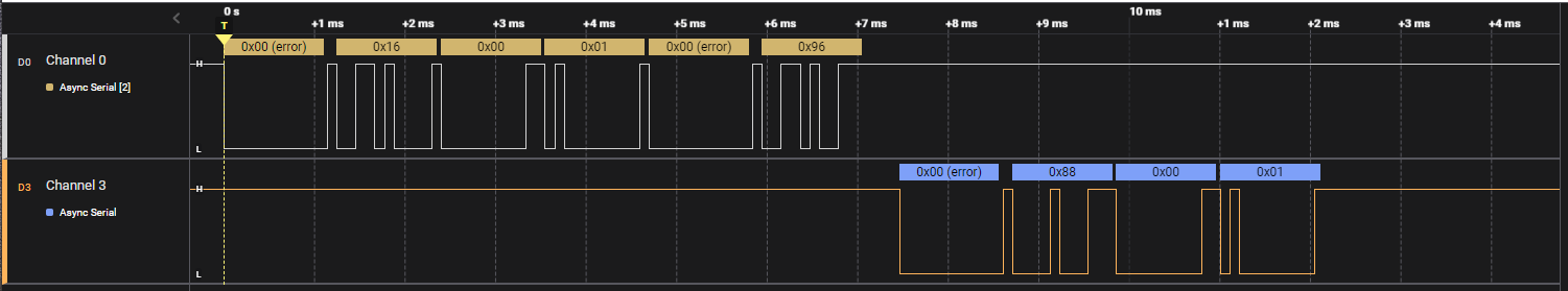
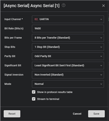
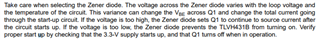
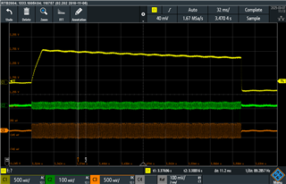
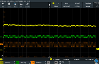
I am trying to talk to AFE881H1 using UBM mode. My goal is to make the reg mode bit one by sending 0x16 0x00 0x01 after sending the break command and then read it back. I think I am complying with the Uart character structure. I am throwing you the image of the message I sent to you in the logic analyzer. Uartout shows a value like 2.7V continuously. is this normal? It did not change when I sent the read command. I read a value like 0x55 continuously.

Please help me with this issue.

  • Yusuf,

    I'm not sure why your UARTOUT is repeatedly sending a signal. However, this is how you should see the transaction on the for writing the 0x01 to register 0x16: 

    After the write to the register, I would immediately follow with the break and the register read. Duplicate this transaction, check the timing, and let me know if that helps.

    Joseph Wu

  • Hello again,
    I tried but I didn't get a response even though I sent the same data. Uartout data still comes with errors. Do you know why this is happening?
    I leave the graph I got from Logic Analyzer.

  • Are your analyzer settings like this?


    And I am sending 11bit low with this function. Is that correct?

    void Send_UART_Break(void)

    {

    while (!(huart2.Instance->ISR & USART_ISR_TXE));

    huart2.Instance->RQR |= USART_RQR_SBKRQ;

    }

  • I can't make sense of the UARTOUT output. I see data after powering the card.
    My hardware connections are as follows;
    UART TX - UART IN
    UART RX - UARTOUT
    ALARM - 3.3V
    CS - 3.3V
    RESET - 3.3V
    REF_EN - 3.3V
    IOVDD - 3.3V
    RTS - 3.3V
    SDI - GND
    SCLK - GND
    CD - IDLE
    CLK_OUT - IDLE
    VDD - GND

  • Yusuf,

    I'm not sure what the issue is. The first thing that I think you need to debug is the UARTOUT line. It shouldn't be continuously broadcasting a signal. Is the device receiving a HART signal at the time?

    Do you have a schematic for your board? I want to see how the device is connected and how it might be set up.

    Joseph Wu

  • Joseph Wu,

    I added the circuit diagram I used. I removed R55, C51, R54, R50 because I thought it might be from the HART signal input. However, I could not change the UARTOUT output. I am adding the data I received from the UARTOUT output. I do not know what else could be the reason.

  • Yusuf,


    When you first power on the device, is the UARTOUT active sending data? Does it start after a specific time after power up?

    When I look at the output it looks to me like the output is really coming out at 19200 baud and repeatedly sending FF. This isn't something that's coming from the AFE881H1, which only has options for 1200 baud and 9600 baud UART.


    Joseph Wu

  • Thank you for your help. I found the problem. I had connected the VREFIO pin directly to GND. When I put 100 nf, it was solved. It was collapsing the voltage coming to the IC. Now I got this data. The only difference from yours is that 0x89 data comes instead of 0x88. What is the difference? Also, why is the RX_INF pin connected to GND with 680pf? What happens if it is not connected? I couldn't understand this. Can you help me?

  • Also, in the sample application the TLVH431 gets very hot. Is this normal? Is the 3.3V in the circuit the same as the 3.3V on my board? I connected it to the 3.3V I made. Is this wrong? How can I change this if I want to power the board with the 3.3V I made instead of external power?

  • Yusuf,


    I'm glad that you were able to find the short from VREF to ground. Hopefully the problems you find become a bit easier.

    I don't think the difference in the first byte from 0x88 to 0x89 is a serious problem. This is the LSb of the status byte. I think it's the R/IRQ bit in UBM mode shown in the Status Bits section in 7.5.4 on page 67.


    Joseph Wu

  • Yusuf,


    The amount of current going to the TLVH431 should not be enough to get the device hot. In fact the power up current for the entire board should start out at exactly 3mA. What amount of current are you measuring in the loop? Can you show a BOM with the resistor values and the exact components you used?

    The RX_INF pin should be connected through a 680pF capacitor to ground. This capacitance is used as part of the internal filtering for the HART signal. I'm not sure what happens if it is directly connected to ground. For now, it seems that you have other problems in setting up the device as part of a transmitter, so I would start by debugging the schematic. How much current is going into the board from the loop and what is the voltage from the TLVH431? What's the voltage across the 3.6V zener diode? What is the base voltage at Q5


    Joseph Wu

  • Yusuf,

    Also /ALARM should not be connected directly to the 3.3V supply. This is an open-drain connection to the pin as an active-low output. This means this should be a resistor pull-up to the 3.3V supply. I'd use a 10kΩ-100kΩ resistor.

    Joseph Wu

  • Thank you very much again for your help.
    I connected the alarm pin to 3.3V with 100K.
    Although the starting circuit needs 3.3V, I see that it produces 1.66 V. When I remove the Q2 transistor in the image I throw, I see that the diode is worth 3.9V. (I didn't have a 3.6V zener, I put 3.9v). When I activate Q2 again, I see the value of 2.25V here. Q2 should form 3.3V.
    Different values ​​from sample application:
    I used 39 or 39k instead of 40.2 or 40.2k.
    Vout output 10k+82k = 92k. The sample was 100 thousand in the circuit.
    499K 470K instead of mode output.
    3.6V Zener instead of 3.9V zener.
    8.2 ohm 10 ohm instead of resistance
    560 ohm instead of 510 ohm. The folding rate here is about 57 instead of 60.
    I put 270 thousand resistance instead of 249k.
    These are differences in the circuit. I think these differences will only change the cycle current, but small differences can be optimized. Because I didn't have certain values.
    I have a hardware error that I cannot foresee.

  • I forgot to mention. I connected the RX_INF pin with 680pf.

  • Yusuf,

    The correct power up of the board depends on the device selection. In particular, that 3.6V Zener diode is an important selection. In the AFE881H1 datasheet, there is a section on the start-up circuit. Here's the schematic shown:

    The Zener must be high enough to turn on Q1 and then pull current through the TLV431B. However, after the TLV431B rises to 3.3V, then the Zener diode must be low enough so that Q1 turns off while Q2 takes over the load. The data sheet says:

    Again, the Zener selection is important. Generally, the Zener would be a high-knee diode, that turns on quickly and gets to the proper voltage.

    I would also check to see if you have other devices on your board taking extra current. 

    Joseph Wu

  • I changed the circuit to this after I couldn't succeed with the startup circuit. I also changed the zener. I installed a 3.6v zener one by one. However, 3.3V always remains between 1.6V-1.7V. Q1 remains in conduction and I could not fix it.

    3.3V comes from the regulator in my own stage. That's why I have a fixed 3.3V. How can I control the output current?

  • Additionally, when power is applied, does the DAC output default to 0.3V?

  • I send 0x0000 as DAC Code. Then when I measure between Vout and ground, I see a value of about 1V. When I send FF, I see 3.3V. Shouldn't I see 0.3V and 2.5V in default mode? Or should I not take the 'visual' as a reference? Note: RX_INF pin is connected to the 'visual' with 680pF

  • Yusuf,


    When the device starts up, the DAC output should be at 0.3V. Even if the device comes up in an error condition, there is an internal circuit that should put out a voltage very close to 0.3V. When you set the DAC code, the output should go from 0.3V to 2.5V linearly from codes 0x0000 to 0xFFFF.

    One of the other things that I also would check is to measure the VREFIO voltage. Your schematic shows that the device has the internal reference enabled, so the reference voltage should come up at 1.25V.

    I would note that the startup current is still not working correctly. Because this section isn't biased correctly, there may be more current being drawn through this section, and loop current may be larger than expected.


    Joseph Wu

  • Thank you for your help. I got the DAC section working. I started working on HART communication. I connected the RTS pin to 3.3V as hardware. There is no pin I can use on the processor. Can't I use HART without using the RTS pin? Would it be enough if I made HART enable from MODEM_CFG?

  • Yusuf,

    The /RTS is used to enable the modulator output. You would normally use this to send a HART transmission. However, you can use the SPI write to the MODEM_CFG register to set the RTS bit to 1. This also turns on the modulator for a HART transmission.

    Joseph Wu

  • Dear Jsoeph,

    I am trying to communicate like this.

    1- Set level 4 from FIFO_CFG
    Sent data 0x0F 0x00 0xF4
    2-Enable HART.
    Sent data 0x0E 0x00 0x48
    3- Set RTS bit low with SPI
    Sent data 0x0E 0x00 0x49
    4-Write data to FIFO_U2H
    Sent data 0x15 0x01 0x99
    Repeat as many times as the number of data
    5- Set RTS bit HIGH with SPI
    Sent data 0x0E 0x00 0x48

    I am watching the Mod Out output with an oscilloscope. I could not see a frequency change, I see a signal with a frequency of 1200Hz.

  • Update
    It sends the data once. However, it continues to send signals at a fixed frequency of 1200 khz. I send the data 0x0E 0x00 0x40 and disable HART, but it still sends signals at 1200 khz.

    Also, I have selected the accept answer option since you solved the problem above. Do I need to open a new conversation for these questions?

  • Yusuf,


    I think the general sequence you listed in your previous post is correct, but there is one issue that I see. For the U2H level set, you wrote: 0x0F 0x00 0xF4. It think this should be 0x0F 0x00 0xF1. For the U2H level, there are only four bits for 32 registers, and the level is represented as the MSb. When the bits of the U2H level are 0b0100, this represents a level of 8. Additionally, the IRQ trips when the level is greater than the value. With a setting of 8, the IRQ trips at 9.

    For your case, I think you would set the bits to 0b0001, which represents a level of 2, and trips when there are 3 bytes in the FIFO.


    Joseph Wu

  • Joseph,
    Hela again. I send data to set fifo level
    0x0F 0x00 0xFF. Then I enable HART.
    I set RTS bit to 1. Then I create a 32 byte array. I send each byte in the following format.

    for (uint8_t i = 0; i < len; ++i) {
    uint16_t fifo_u2h = data[i]; // Add data bits
    fifo_u2h |= (CalculateOddParity(data[i]) << 8);
    // Write to FIFO buffer
    AFE881H1_WriteRegister(AFE881H1_FIFO_U2H_WR_OFFSET, fifo_u2h);
    }
    The loop sends data to U2H_WR in the format 0x15 0x1 0xFF. (All data is set to 0xFF)
    After this loop is complete, I set the RTS bit to 0.
    When I look at the Mod Out output with an oscilloscope, I see the following signal.


    There seem to be 32 registers sent, but when I examined the data in detail, I could not see any meaningful data. I am sharing the data I received with you. What causes this?


    Also the last 2 registers are different from the others. Do you know why?
    Thank you for all your help.

  • Yusuf,

    I'm not sure what all of your transmission is doing, but it looks like some of it is correct. For example this was one of your plots from the last post:

    Here you can see that the device starts the modulator, and then sends a start bit of 0. After that, it looks like the data is FF, presumably followed by the parity bit and stop bit, which both happen to be 1.

    In the last plot, I'm not sure what the last two bytes are, but it looks like a similar transmission, except the data is 0F instead of FF. 

    I think if you change the data in the transmission, you'll be able to see more variation in signal. Maybe sending 0xF7, you'll see the last 1, the odd parity 0 and then the 1 stop bit. 

    One final thing I wanted to send you was that there is an app note on basics of HART. It might have some information to help you review the signals.

    https://www.ti.com/lit/pdf/SLAAEH0

    Joseph Wu

  • Dear Joseph,

    Thank you. I have obtained an oscilloscope image that I can send the correct data. I have verified the data. . Below is the image of the oscilloscope image I added, LOOP -, LOOP+ and 2.2nF output. I see that the signal I send also comes to the RX_IN pin. I feed it with a DC source by giving 5V. At the same time, I saw that my own data returns to the RX_IN pin. The capacitor output is a little different. I observe my correct signal?
    Note: yellow   --> 2.2nF output
              Orange --> LOOP-
              Green  --> LOOP+

    My second question is, if I connect two afe881h1s together and want to transmit from one and receive from the other, how can I do this? If I connect the LOOP+ and LOOP- values ​​of the two circuits together, will this method be correct?

    I am also adding a photo of my circuit.

  • Yusuf,

    Just a quick look at the HART signals makes me think that the signal is correct. It seems to be sending current through the loop and you presumably have a resistance that is used to turn the sinusoid to a voltage. 

    Normally, you wouldn't connect two AFE881H1 devices together to talk to each other. The device is meant to be the center of a HART enabled field transmitter. In that case you would have a HART controller talking to the transmitter. Additionally, you can think of the AFE881H1 device as a current controller through the loop, and you wouldn't normally have more than one current control on the loop.

    However, you might be able to set up the device in a multidrop mode so that these devices are paralleled together. It's set up in this way:

    If you don't have the HART controller, but do have some ability to send commands through an AFE881H1 device, you can use the same sense resistor for the communication from both devices. This would test the transmission on one device and the reception on another.

    One other app note that may be useful in your testing HART on a field device is the following:

    http://www.ti.com/lit/pdf/slaaeh8

    Joseph Wu