Other Parts Discussed in Thread: ADC3644, ADC3643, , THS4541
Tool/software:
Dear Technical Support Team,
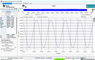
I installed HSDC v6.0, but it doesn't include ADC3644.
If I need to install patch, could you provide it?
Best Regards,
ttd

Tool/software:
Dear Technical Support Team,
I installed HSDC v6.0, but it doesn't include ADC3644.
If I need to install patch, could you provide it?
Best Regards,
ttd