This thread has been locked.

If you have a related question, please click the "Ask a related question" button in the top right corner. The newly created question will be automatically linked to this question.

ADS131M06: ADS131M06

Part Number: ADS131M06
Other Parts Discussed in Thread: ADS131M08EVM, ADS131M08

Tool/software:

We use a lot of TI products, especially mmwave and ADS112U04IPW . We are using the ADS131M06 with the older MSP430GF4619 which we have a lot of experience with using SPI, SCI and many other features. We are stumped trying to simply read the 6 Analog ports from the ADS131m06. Configuration registers are straight forward.

RREG (101a aaaa annn nnnn) 1010 0000 0000 0110 //READ starting from register 0 7-1 bytes

Assuming default start up gain=1, 24bit data, and other default conditions so it auto converts.

void ADS131_readConversion() { //read all 6 channels into array
IO_LOW(P9,BIT7); // Chip Select ADS13
for (int ch = 0; ch < 6; ch++) { // Read 6 ADC channels
command = 0XA | (ch & 0x07); //THIS DOES NOT LOOK CORRECT?? RREG (101a aaaa annn nnnn) 1010 0000 0000 0110 //READ starting from register 0 7-1 bytes
while (!(IFG2 & UCB0TXIFG)); // Wait for TX buffer ready
UCB0TXBUF = command; // Transmit the command byte
while (!(IFG2 & UCB0RXIFG));ch = UCB0RXBUF; // Wait for transmission and clear RX flag with a dummy read
unsigned int high = SPI_transfer(0x0000); //read lo, mid, hi byte
unsigned int mid = SPI_transfer(0x0000);
unsigned int low = SPI_transfer(0x0000);
adc_data[ch] = ((unsigned long)high << 16) | ((unsigned long)mid << 8) | low;
} // Read 6 ADC channels
IO_HIGH(P9,BIT7); ; // Deselect ADS131
}

We have read countless examples of the code and the user manual but it is not clear

WHERE ARE REGISTERS FOR THE 24BIT DATA?

ARE ANY OTHER STARTUP COMMANDS NEEDED?

DO WE NEED TO SEND THE READ COMMAND AND ADDRESS EACH A/D CHANNEL 0XA | (ch & 0x07);

PLEASE HELP WITH THE CODE ABOVE.

Many thanks, Peter

  • Hi peter mccormick,

    Can you provide us logic analyzer plots showing the communication to and from the ADC? Please include CS, DOUT, DIN, DRDY, SCLK, and SYNC

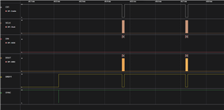
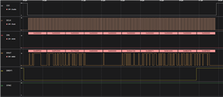
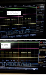
    Below is how the ADS131M08EVM operates: you can see that when you are ready to take data, the SYNC pin is toggled to resynchronize conversions. Then, once DRDY drops low, the data is clocked out by sending SCLKS (nothing on DIN, see second image).

    In the second image you can see that 10 words are clocked out (response, 8x data, CRC). The M06 will have 8 words because there are two fewer channels

    This is how I would expect your system to operate, please share similar captures of your system behavior so we can review

    -Bryan

  • Hi Peter,

    thanks for trusting TI with your ADC needs and your interest in ADS131M06.

    In ADS131M06, the conversion data are not stored in any user registers. Means you can't use the RREG command to read them.
    The ADS131M06 always outputs the conversion data on DOUT, unless you sent a RREG command to read more than one register.
    That means in the default configuration you would simply send a frame with 3 x 8 x 8 = 192 bits, where DIN is held at 0 (=NULL command).
    This will output eight 24-bit wide words. Within each 24-bit word the data is left (MSB) justified.
    The first word includes the 16-bit response, words 2 to 7 include the 24-bit conversion data for the six ADC channels, and word 8 includes the 16-bit CRC.

    Regards,
    Joachim Wuerker

  • The first word is the 16 bit response to what command?

    Will DOUT start sending channel 1,2,3,4,5,6,1,2.... as we send it 00 frames?

    I understand that The default is no CRC which is OK for us.  How do we know when Dout is channel 1 if Dout is constantly sending channel data?
    Is it the Sync line or do we send a Reset then start sending.  We will send some SPI traces if this does not work. 

    Are there any commands we need to send it to immediately send data?

    We appreciate your help. thanks

  • Hi peter mccormick,

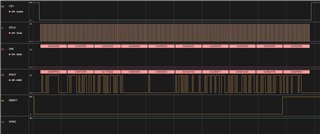
    I copied my logic analyzer capture again for reference:

    • You can see that there is no command being sent - just SCLKs - to read out the data
    • As mentioned, the first 24-bit word is the response from the previous command, the next 8x words are the data from each channel (Ch0, CH1,... Ch7, again I used the ADS131M08 for these tests), and the last word is the CRC. See Figure 8-18 for a typical communication frame
    • The response in this case is the STATUS byte because the previous command was the NULL command. See Table 8-11 for more info
    • The default is no CRC on the input (DIN), the CRC is always on the output (DOUT) however
    • The response and CRC are both 16-bit, with the last 8 bits = 0 because the word length is 24-bit

    You should use DRDY as an interrupt to determine when to read data. The EVM flow for capturing data is:

    1. Send the SYNC pulse
    2. Wait for DRDY to transition high to low
    3. Drop CS low and keep DIN low
    4. Send as many SCLKs as necessary depending on the word size you select. The default word length is 24-bits, which requires 8x24 = 192 SCLKs using the ADS131M06
    5. Bring CS high
    6. Repeat steps 2-5 as many times as necessary to continue clocking out data

    -Bryan

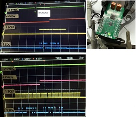
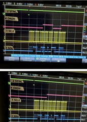
  • Attached are the scope plots. Thanks, Peter
    ===Sync/Reset goes low but /DRDY takes .5mS to go low. Waiting on /DRDY even for extended time does not help.
    ===How long should /DRDY take after /SYNC ?
    ===I am not configuring any setup registers. Does a register need be configured first?
    ===Is first SPI_transfer(0x00) in code below needed to prepare to read AD0
    ===The 6 results=4286677119 4294741376 72792 7307266 4286578815 4294741376 even with input at 0V or 1V so something is wrong.


    void ADS131_read(void) { int jj; //read all 6 channels into array. Assuming default start up gain=1, 24bit data, and other default conditions so it auto converts.
    unsigned int byteHigh, byteMid, byteLow; unsigned long result;
    IO_LOW(P9,BIT4);longdelay(2); IO_HIGH(P9,BIT4); // reset to sync data
    jj=0; while((P9IN & BIT5)&& jj++<100); //if(jj>90) { user_debug_msg("AD NOT READY"); } //wait for Data Ready to go low
    IO_LOW(P9,BIT7); // Chip Select ADS13
    //SPI_transfer(0x00); //??????? send an empty command and read response to initiate the transfer.
    for(jj=0;jj<6;jj++) { //read 6 channels
    byteHigh = SPI_transfer(0x00); // Dummy write to read high byte
    byteMid = SPI_transfer(0x00); // Dummy write to read mid byte
    byteLow = SPI_transfer(0x00); // Dummy write to read low byte
    result = ((long)byteHigh << 16) | ((long)byteMid << 8) | byteLow; // Combine the three bytes into a 24-bit result
    if(result & 0x800000) { result |= 0xFF000000; } // Perform sign extension if the ADC uses two's complement format
    a_d[jj]=result; //put result into array
    } //read 6 channels
    IO_HIGH(P9,BIT7); ; // Deselect ADS131
    } /read all 6 channels into array.
    //---------------------------------------------------------------------
    // SPI_transfer Transmits one byte over SPI and returns the received byte.
    unsigned int SPI_transfer(unsigned int data) {
    while (!(IFG2 & UCB0TXIFG)); // Wait until TX buffer is ready
    UCB0TXBUF = data; // Send data
    while (!(IFG2 & UCB0RXIFG)); // Wait for reception to complete
    return UCB0RXBUF; // Return received data
    }

  • Attached are the scope plots. Thanks, Peter
    ===Sync/Reset goes low but /DRDY takes .5mS to go low. Waiting on /DRDY even for extended time does not help.
    ===How long should /DRDY take after /SYNC ?
    ===I am not configuring any setup registers. Does a register need be configured first?
    ===Is first SPI_transfer(0x00) in code below needed to prepare to read AD0
    ===The 6 results=4286677119 4294741376 72792 7307266 4286578815 4294741376 even with input at 0V or 1V so something is wrong.


    void ADS131_read(void) { int jj; //read all 6 channels into array. Assuming default start up gain=1, 24bit data, and other default conditions so it auto converts.
    unsigned int byteHigh, byteMid, byteLow; unsigned long result;
    IO_LOW(P9,BIT4);longdelay(2); IO_HIGH(P9,BIT4); // reset to sync data
    jj=0; while((P9IN & BIT5)&& jj++<100); //if(jj>90) { user_debug_msg("AD NOT READY"); } //wait for Data Ready to go low
    IO_LOW(P9,BIT7); // Chip Select ADS13
    //SPI_transfer(0x00); //??????? send an empty command and read response to initiate the transfer.
    for(jj=0;jj<6;jj++) { //read 6 channels
    byteHigh = SPI_transfer(0x00); // Dummy write to read high byte
    byteMid = SPI_transfer(0x00); // Dummy write to read mid byte
    byteLow = SPI_transfer(0x00); // Dummy write to read low byte
    result = ((long)byteHigh << 16) | ((long)byteMid << 8) | byteLow; // Combine the three bytes into a 24-bit result
    if(result & 0x800000) { result |= 0xFF000000; } // Perform sign extension if the ADC uses two's complement format
    a_d[jj]=result; //put result into array
    } //read 6 channels
    IO_HIGH(P9,BIT7); ; // Deselect ADS131
    } /read all 6 channels into array.
    //---------------------------------------------------------------------
    // SPI_transfer Transmits one byte over SPI and returns the received byte.
    unsigned int SPI_transfer(unsigned int data) {
    while (!(IFG2 & UCB0TXIFG)); // Wait until TX buffer is ready
    UCB0TXBUF = data; // Send data
    while (!(IFG2 & UCB0RXIFG)); // Wait for reception to complete
    return UCB0RXBUF; // Return received data
    }

  • I tried again to make it work again.  It seems close.  The DRDY does not behave properly.  

    I also tried this to no avail:   long RESET.  waiting for DRDY to go high before SYNC.  reading many frames before sync to try to flush the buffer

    DRDY randomly goes high after 2 frames or randomly at other intervals.  DIN is low.  Output results not consistent.  We use SPI for Flash also.

    DRDY does not go high after reading 8 frames.  Below is the code.========================================

    void ADS131_read(void) {    int jj; float fresult;     //read all 6 channels into array.       Assuming default start up gain=1, 24bit data, and other default conditions so it auto converts.

    #define ADSCALE_TO_VOLTS  0X7FFFFF    //7FFFFF=1V        7FFFFFh = positive full scale    800000h = negative full scale

    #define WAIT4RDY 30000  //10 words are clocked out (response, 8x data, CRC).  DIN must be low 

         unsigned int byteHigh, byteMid, byteLow;     unsigned long result;

         IO_LOW(P9,BIT4);longdelay(2); IO_HIGH(P9,BIT4); //Sync

         IO_LOW(P9,BIT7);                             // Chip Select ADS13

         SPI_transfer(0x00);                          //dummy read initial command response

         for(jj=0;jj<=6;jj++) {                        //read 6 channels

                byteHigh = SPI_transfer(0x00);        byteMid  = SPI_transfer(0x00);      byteLow  = SPI_transfer(0x00);        // Dummy write to read low byte

                result = ((long)byteHigh << 16) | ((long)byteMid << 8) | byteLow;  // Combine the three bytes into a 24-bit result

                if(result & 0x800000) { fresult = (float)((unsigned long)result & 0x7FFFFF); fresult=fresult-0x7FFFFF; } // max negative = 800000 .   FFFFFFh = slightly negative    0h=0V

                else fresult=result;                       //result positive

                a_d[jj]=fresult/ADSCALE_TO_VOLTS;          //put floating point voltage into array

        }                //read 6 channels

        SPI_transfer(0x00);  //read CRC.  do not check it

        IO_HIGH(P9,BIT7); ;   // Deselect ADS131        

    }

  • Hi peter mccormick,

    What is your SCLK speed? It looks like in your first scope shot that it takes 8 divisions at 200ua/div, or 1.6ms, while in the second scope shot it seems like it takes 5 divisions at 500us/div, or 2.5 ms. Is the SCLK speed changing?

    And I am assuming there are 24 SCLKs in each of those (again, a logic analyzer would be very helpful in this case)?

    It is possible your are not retrieving data fast enough and therefore it is getting overwritten. This would explain the odd DRDY behavior. As you can see from my initial logic analyzer plots, the time division is 100us, and the entire data transaction is ~10% of that entire time, or ~10us.

    -Bryan

  • We continue to try to make this work.  You can see the logic analyzer is working in the 4 X 24 clock plot. The uC is correctly reading the values so SPI works.   DRDY always goes high after 3X24 clocks.  Clock is 392kHz.  

    DRDY is already low when we randomly do the SYNC.   It only goes high after the 3rd frame.

    Why does DRYD always go high after the 3rd frame?

    If we get it to work, are the 6 channels in frames 2-7  ?  thanks 

  • Hi peter mccormick,

    What data rate are you operating at? Are you just powering up the ADC and sending data, such that all registers are at the default values?

    And what is the ADC clock speed that you are providing to the device?

    -Bryan