This thread has been locked.

If you have a related question, please click the "Ask a related question" button in the top right corner. The newly created question will be automatically linked to this question.

ADS1278EVM-PDK: Interfacing ADS1278EVM-PDK (standalone with out the PHI controller) with FPGA

Part Number: ADS1278EVM-PDK
Other Parts Discussed in Thread: ADS1278, ADS1278-SP, MSP430FR5969

Tool/software:

Hello everyone,

I am using the ADS1278EVM-PDK evaluation board to prototype a data subsystem for the ADS1278-SP ADC chip. For our data system, we plan to interface the ADS1278 chip with an FPGA board using the frame-sync protocol, as this approach provides a deterministic state machine—especially important since I intend to switch the external analog input after each sample.

Initially, I controlled the EVM through the PHI controller using the ADS1278 GUI and captured signals (DOUT1, SCLK, FSYNC, CLK) with an oscilloscope to verify timing diagrams and confirm my understanding based on the datasheet.

Next, I plan to interface the EVM using my own FPGA design without the PHI controller. Before proceeding further, I would greatly appreciate feedback from TI engineers and the community regarding my hardware and configuration setup outlined below.

Hardware System:

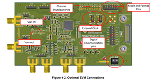
Due to limited available I/O, I will use only one of the eight channels. An external analog multiplexer (MUX) will eventually switch the input signal. Currently, I'm using a stable 1.5 V DC signal for initial testing.

1. Disconnect the PHI controller connector from the EVM.

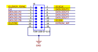
2. Solder pin headers onto the unused PWDN pins and use jumpers to disable unused channels (the corresponding PCB holes are unpopulated).

3. Tie the configuration pins to GND or 3.3 V as specified by my intended configuration.

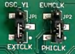
4. Select EVMCLK using the onboard oscillator OSC_Y1

5. Use the EVM's provided 6 V supply connector for power.

Configuration:

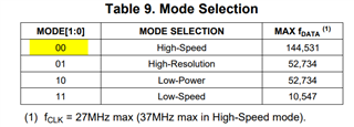
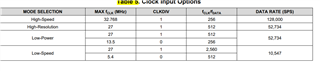
  • Mode: High-Speed (using the onboard 27 MHz oscillator initially; we may maximize Fclk later if needed).

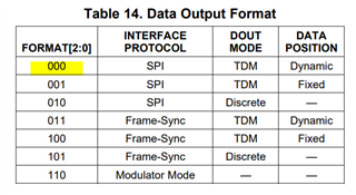
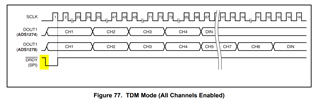
  • Frame-Sync, TDM, Dynamic mode (PWDN = 1 for the active channel, 0 for unused channels).
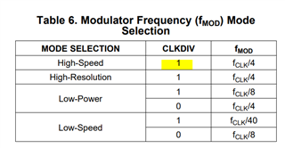
  • CLK_DIV set to 1.

  • Test mode disabled.

I/O

  • SYNC: Synchronization (initial reset)

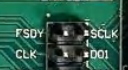
  • FSYNC, DOUT1, CLK, SCLK for Frame-Sync communication

  • CLK to SCLK ratio = 1

FPGA logic:

1. Pull SYNC low for at least one CLK cycle (currently using two cycles).

2. Generate 128 FSYNC periods (each FSYNC period consists of 256 CLK cycles, 50% duty cycle) to prepare data conversion.

3. Start reading data at the beginning of the next FSYNC cycle. Sample data on the rising edge of SCLK since data shifts out on the falling edge.

**Question:

  1. Does my hardware and FPGA setup appear correct?

  2. What is the recommended power sequencing between the FPGA board and the ADS1278EVM-PDK? Should the FPGA board power on first, or vice versa? If the FPGA must be powered first, I'll add logic to prevent automatic FSM startup.

  3. Must I assert the SYNC signal and then wait another 128 FSYNC cycles every time I switch the analog input after each sample? I must switch the input signal as all input signals represent different science data.

  4. Is an FPGA necessary for interfacing with the ADS1278-SP chip, or can an MCU such as the TI MSP430FR5969 achieve the same performance? Given the limited pins on the mission main processor, any recommendations for alternative interfacing methods would be welcome.

Thank you in advance for your guidance and feedback!

  • Hello Yuchen,

    I included a detailed list of changes needed to use the ADS1278EVM stand-alone below.  I would suggest using SPI mode for communications; this will allow f-CLK up to 27MHz, supporting data rates up to 105Ksps.  In addition, at this data rate, you can use a single DOUT for all 8 channels in TDM mode. Also, using all 8 channels is preferable to using a single channel with a multiplexer to eliminate the settling time of the internal digital filter.

    You can also use frame-sync mode, but you will need an MCU that can support this protocol or an FPGA; many general purpose MCU's do not directly support frame-sync.  The main advantage of frame-sync is that it supports data rates up to 144Ksps (128Ksps for the ADS1278-SP) and SPI is limited to 105Ksps.

    Steps 1 through 3 above appear correct.  In Step 4, in order to use the EVM's on-board 27MHz oscillator, you need to move jumper JP1 to the 27MHz (OSC_Y1) position and jumper JP2 to the EVMCLK position.  The rest of your configuration looks correct for frame sync.

    Questions/answers:

    1.  Yes,

    2.  If there are voltage levels present on the digital inputs of the ADS1278 before power-up, the ADS1278 may not work correctly.  You should power-up the ADS1278EVM first, and then your FPGA board.

    3.  No, but you will have a settling time.  Whenever there is a step change in the input signal, the internal digital filter will require 76 conversion cycles to settle to the new input level.  Since you are controlling the external multiplexer, after an input channel change, wait 76 conversion periods, and then read the data.  The other option is to use all 8 channels of the ADS1278 instead of an input multiplexer, assuming 8 input channels is enough for your system requirements.

    4.  Yes, a standard MCU with SPI can easily interface to the ADS1278.  As I had mentioned before, you can support up to 105Ksps per channel, and TDM all 8 channels over a single DOUT line (DOUT1).  This is how most folks use the device.

    Regards,
    Keith Nicholas
    Precision ADC Applications

    How to use an external MCU with the ADS1278EVM

    Here is the list of changes needed to use the ADS1278EVM stand-alone with SPI.

    In order to use the ADS1278EVM board with an external controller, you need to remove the PHI board, otherwise, the digital lines will be driven by the PHI board preventing correct operation with an external MCU.

    1.  Provide +6V on J10 from an external bench supply.

    2.  Move jumper JP1 to the 27MHz position, this enables the on-board 27MHz oscillator.

    3.  Move jumper JP2 to the EVMCLK position, this selects the on-board 27MHz oscillator.

    4.  You may need to install jumpers on J4, depending on the mode of operation that you want to use.  For example, configure ADC for high-speed, SPI, TDM, Dynamic, then you will need to install jumpers on MODE0, MODE1, FORMAT0, FORMAT1, and FORMAT2.  CLKDIV should remain open (high).

    For the SPI connections on J6:

    1.  MISO -> DOUT1

    2.  SCLK -> SCLK

    3.  Connect DIN to GND, do not leave floating.

    4.  Connect /SYNC to an IO pin on your MCU (needed for robust power-up reset), or tie to IOVDD for test purposes.

    5.  Connect /DRDY to an IO pin your MCU.  This is an output from the ADC, indicating when data are ready to be read.  The code should monitor this pin (polling or interrupt) and only transfer data after a falling edge (Figure 77).

  • Hello Keith,

    Thank you for the detailed response. I calculated the time required to complete one round of data collection, and based on my results, it seems that I may not be able to achieve the mission's targeted data rate. According to the datasheet, enabling the modulator output mode allows bypassing the digital FIR filter. Can I use this mode for data collection? Does the modulator output provide the final converted data, or is additional post-processing required?

  • Hello Yuchen,

    Yes, you can use modulator mode, but you must create a suitable digital filter in your processor.  Please note that you will need to sample data at the modulator data rate, which is f-CLK/4 for high speed mode, or 6.75MHz when using f-CLK=27MHz.

    Would it be OK if we reached out to you at your email address for your myTI account?

    Regards,
    Keith

  • Yes. It is OK to reach out to me through my registration email. Thank you for helping, and I will have more questions regarding this ADC for sure.

  • O.K.  If you have more ADS1278 questions, you can reply to this thread or create a new thread.

    Regards, Keith