This thread has been locked.

If you have a related question, please click the "Ask a related question" button in the top right corner. The newly created question will be automatically linked to this question.

ADS1261: Responding with All Zeros

Part Number: ADS1261

Tool/software:

TI-ADS1261 ADC is always transmitting bytes with a value of zero over SPI bus back to master.

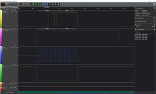
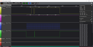
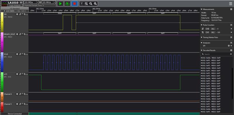
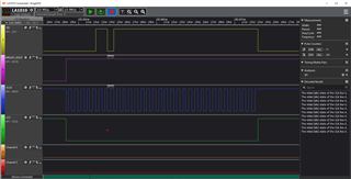
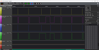
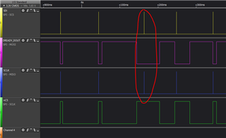
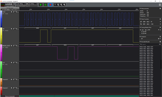
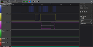
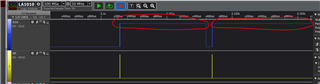
TI-ADS1261 Analog to Digital Converter is connected to Xilinx Zynq 7020 SOC (System On a Chip) through the Zynq SPI Bus Serial Interface. Pins used for communication are CS (Chip Select), SCLK (Serial Clock), DIN (Data Input) and (DOUT/DRDY) Data Output / Data Ready. SLCK is running at 33 MHz / 512 = 65.104 KHz with a period of 15.36 Microseconds. 

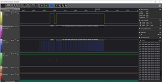
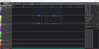
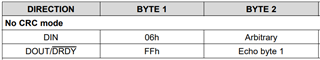
The correct number of bytes is transmitted by the ADS1261 in response to commands and read registers but the value of all bytes is zero. For instance sending a reset command - 0x06, 0x00, 1261 responds with 0x00, 0x00 instead of 0xFF, 0x06. Or sending RREG of Status Register = 0x21, 0x00 1261 responds with 0x00, 0x00, 0x00 instead of 0xFF, 0x21, <Status Register Value>. 

My hardware engineer placed a scope on the SCLK, DIN and DOUT. Clock looks good, DIN is being correctly driven by Zynq SPI and DOUT is being driven by 1261 with bytes that are serial zero for every byte.

Our software is initializing as follows.

Reset SPI, First initialize the SPI Bus system clock, interrupts, configuration register, Reset SPI. as follows:

Xilinx SPI Configuration Register CR = 0x0000FC35

// Bit 17 = 0 ModeFail Generation Disable
// Bit 16 = 0 Manual Start Command
// Bit 15 = 1 Manual Start Enable
// Bit 14 = 1 Manual Chip Select Mode
// Bit 13:10 = 1111 No Slave Selected
// Bit 9 = 0 Peripheral Select decode Only 1 0f 3 selects
// Bit 8 = 0 Use SPI Reference Clock
// Bit 7:6 = 0 Reserved
// Bit 5:3 = 110 Baud Rate Divisor Divide by 128
// Bit 2 = 1 Clock phase SPI clock is inactive outside the word
// Bit 1 = 0 Clock Polarity outside SPI word SPI Clock is quiescent low
// bit 0 = 1 Mode Select SPI is in Master Mode

Then we use the initialized SPI bus to initialize the TI-ADS-1261 as follows:

Send command reset, read status register, write all registers with default values.

TI-ADS-1261 responds to reset command and all write register commands with all zeros.

We are using the TI-ADS-1261 as our ADC for reading various critical voltages in real-time from our hardware.

Any help in getting the TI-ADS-1261 up and running, much appreciated.

  • Hi Everett Everett,

    Can you please provide logic analyzer captures showing the complete data transmission during your data readback? Please include CS, DOUT, DIN, SCLK, and DRDY

    Please also provide a schematic

    -Bryan

  • Bryan,

    Hi. Thanks for responding so quickly. I will get you those logic analyzer plots for the four SPI comm pins as soon as I can. Our logic analyzer needs to be replaced. Would it be helpful here if I listed all my SPI bus register settings I'm using to initialize the bus? I'm initially running the SPI bus at 33.3 MHz with a clock divisor of 4 and a configuration register prescaler divider of 32 which I believe would be 260 kHz. I wonder what clock would be good for the 1261 to initially be happy with it before it's own registers can be written. We are using the same Vivado FPGA from our previous project which has the exact same hardware connections to the Xilinx SOC for SPI CS, SCLK, DIN and DOUT/(not)DREADY. Like I said I'm poling the Xilinx SPI RX FIFO and it is reporting bytes present which are zero when read. I am very carefully following the instructions in Zynq-7000 SoC Technical Reference Manual to program the bus. This is my first time programming the 1261 so I apologize if I'm not asking the right questions.

  • Hi Everett Everett,

    The ADS1261 has no minimum SCLK speed, assuming you are not using the SPI timeout feature. It might be good to try something like 1 MHz however, just to be sure

    If you pull the ADS1261 START pin high, do you see the DRDY pin toggling at ~50 Hz once you have the ADC power and clock established? That is a good indication that the ADC is actually powered and clocked correctly, and the ADC modulator is processing data. If not, then you have an issue with the power (or ground) and/or the clocking)

    Can you send us a schematic as well?

    -Bryan

  • Bryan,

    I think your suggestion here may have solved the problem for us. I asked our hardware engineer where he has the START connected and apparently they ran it into one of the GPIO pins which my software currently does not have access so I am not driving the START pin high. That would perhaps explain why the 1261 is not responding. We are in the process now of going into Vivado and figuring out how we can give my software access to that GPIO line. I will post again in a couple weeks after we have that worked out so the results are captured in this thread. Thanks for your help!

  • Hi Everett Everett,

    Thanks for the update.

    For now I will mark this resolved. Of course you can always add more info to this thread, or start a new one if needed

    -Bryan

  • I'm resetting the 1261 using our new pin attached to START. But I'm still not getting any data from the 1261 on the DOUT/DREADY line. I have attached logic capture images. A couple times I got data 0xFF, 0x08 in response to reset 0x06, 0xFF but most of the time I get all zero or all 0xFF. I've tried many different baud rates determined by the Xilinx SPI bus divisor.

  • Hi Everett Everett,

    I had asked if - after a reset - you could pull the ADS1261 START pin high and then monitor the dedicated DRDY pin - do you see this pin toggling at ~50 Hz?

    Also your SCLK is triggering on the wrong edge, it should trigger on the falling edge, not the rising edge. This is not causing the issue you are seeing, but it should be changed either way

    -Bryan

  • Hi. Wow that was fast. My hardware engineer looked at the graphs and agreed with you that the clock edge seems to be out of phase. I can reverse the polarity of the clock easily in the Xilinx SPI bus settings so I will try that right away. I will also pull the START high and do nothing else on the buss and see if the logic an. shows the 50 Hz. This is easy so I will get back in a couple hours with the data.

  • Hi Everett Everett,

    Understood, we will wait for the results of your tests

    -Bryan

  • I just finished the additional tests. If all I do is pull the START pin high I do not see a 50 Hz signal on DRDY or any periodic waveform on it at all. The attached logic analyzer capture is our effort to get the clock polarity correct. However the logic analyzer can no longer decode data and notice the DRDY pin moves but does not appear to contain data. It looks like it is stuck in a DRDY function without changing to DOUT in order to echo the MOSI command of 0x06, 0xFF.

    To get the Xilinx Zynq 7020 SPI bus clock set I am setting the following bits in the Xilinx CR register.

    BIT 2 = 1 // Third bit clock innactive outside word.

    BIT 1 = 1 // Second bit clock quiescent high

    Also I am transmitting extra bytes to keep the SPI Bus open so clock is provided to the 1261 for its response. So my command is actually 0x06, 0xFF, 0xFF, 0xFF. When I only transmitted 0x06, 0xFF the SPI bus would turn off the clock immediately after transmitting the second byte which I thought might be preventing the 1261 from responding.

  • Hi Everett Everett,

    Now SCLK is idling high, which will not work at all. SCLK needs to idle low, and you need to capture data on the falling edge of SCLK. You previously had the SCLK polarity correct

    Are you monitoring the dedicated DRDY pin, or the combined DOUT/DRDY pin? Please check the dedicated DRDY pin only in the test I previously described, you do not need to monitor DOUT/DRDY

    -Bryan

  • OK, I will fix the clock back to what it was. Clock idle low, innactive outside word and capture falling edge. We have the logic analyzer connected to the 1261 DOUT/DRDY pin, the combined pin. I was not aware the 1261 had a dedicated DRDY pin. I will check with our hardware engineer and get him to pin that out and repeat the START test using that pin. Though I'm curious why the 1261 is not putting data on the combined pin. Maybe if I fix the clock that will work, but before it was only doing zeros or all 0xFF and was not echoing the command (as you are aware already).

  • Hi Everett Everett,

    Understood, we will wait for the results of your tests

    -Bryan

  • Hi. Below are the latest logic analyzer captures for SPI clock set to idle low, inactive outside word, data on falling edge. I get nothing on the DOUT line except that with these settings it follows the NOT CS exactly. The first image is a wide view showing the DOUT/DRDY following CS and the second is a closer view showing clock and MOSI from SPI bus to 1261 for the reset command 0x06, 0xFF, 0xFF, 0xFF. For some reason I can no longer get the logic analyzer to decode using these settings. I also discovered that the SPI Bus must be disabled between activity and enabled before transmit and also the SPI clock must be set to innactive outside word otherwise the logic analyzer will capture nothing and everything is flat. The DOUT/DRDY looks like it is stuck in DRDY mode and refusing to go to DOUT mode to transmit data, though of course this is just a wild guess. My HW engineer has not yet pinned out the dedicated DRDY line but we are doing that now so we can check for the 50 Hz you mentioned. Many thanks.

  • Hi Everett Everett,

    Can you clarify how your signals are labeled in the images you sent? Each signal has a written label, and then underneath has an associated label for the SPI analyzer. For example, the first (yellow) signal says "SDI" and "SCS". Since these are in conflict, which is correct? I cannot tell from the signals themselves, other than the blue signal appears to be SCLK

    If the green signal is CS, why are you sending SCLKs and info on DIN when CS is high? The device will not respond to any commands while CS is high. So can you clarify what you are showing me?

    -Bryan

  • You are correct, I noticed the same thing myself this morning, somehow our logic analyzer channels got changed. This should be fixed now in the following diagram. In the same order the channels are positioned in the diagram:

    Channel 1 Blue is SCLK,

    Channel 3 Yellow is SDI MOSI (Master SPI Bus out Slave 1261 In). 

    Channel 0 Purple is DOUT/DRDY (MISO),

    Channel 2 Green is NOT-CS,

    I have the Xilinx SPI bus master set to clock quiescent low, clock not active outside word. In this run I ran the bus in manual mode. In this run I also cycle through all three slaves on the bus sending the reset command to the 1261 using a different slave in an effort to see if I could get chip select to move but nCS is not moving at all. Our HW engineer insists CS is hooked up correctly but it is behaving like the Xilinx SPI bus is not driving it regardless of the register setting for the selected slave. Also as you can see the SPI bus is only driving the clock during transmit which means there is no clock available to the 1261 to respond for the second byte. I'm not sure how to fix this. 

    Also, as you suggested, we hooked up a scope to the dedicated 1261 DRDY pin and only set the START pin and did nothing else and there is no periodic signal on the 1261 dedicated DRDY.

    EDIT: I also reran the test setting clock to active outside word and the bus in automatic transmit mode and the resulting graph is exactly the same, no movement on CS or DOUT.

    I think the first priority is to figure out why the 1261 is not responding to START with DRDY and why the Xilinx SPI bus is not moving CS, though I'm not sure yet how to proceed. Below is the latest plot with the channels set up correctly.

  • Hi Everett Everett,

    Your SCLK is still triggering on the wrong edge in the capture (should be on the falling edge). If that is the case for just the analyzer, then that shouldn't affect the communication, just your captures will be wrong. If the controller is capturing data on the wrong edge however, then the communication won't work.  

    Can you send us a schematic?

    Can you send us pictures of your setup i.e. how is it all connected together?

    Do you have an EVM you could try? This can act as a baseline for your board, so you know what the communication should look like and because the EVM analog / digital circuitry has been tested

    -Bryan

  • Sorry to say we damaged our chip select pin. Which is why all day today with software changes I saw no chip select. We went back to an earlier release with diagrams that clearly show chip select moving and they no longer worked so we checked the CS pin and indeed it was yanked out, probably when we were probing for the dedicated DRDY pin (which is very small). So you're off the hook for a few days while we fix the board. Please keep the issue open since we still need to get DOUT working after the board is fixed. Sorry for the bad information today. 

    I doubt I can get you schematics since this is an ITAR project but I may be able to create a detailed list of connections and your suggestion for the EVAL board makes sense and I will pursue that. More later.

    -Everett

  • Hi Everett Everett,

    Understood, we will wait for further info from you

    -Bryan

  • Bryan,

    Hi. We fixed our board and fixed the CS pin. After doing this and carefully reviewing my software I run the Xilinx SPI bus in Manual Slave Select and Auto Transmit and I get the following graph. This is a huge advancement over before because the 1261 is obviously responding in some way. However in response to the reset command TX 0x06, 0xFF, the 1261 drives the DOUT with 0xC6, 0xFF. The response has two high order bits added changing the 0x06 to 0xC6. My software confirms that it is reading the 0xC6 from the FIFO which matches the logic analyzer decode in the diagram below.

    Also the Xilinx SPI bus is only driving the clock during transmit and I have not yet figured out how to keep the bus clock going for the full 1261 response, but this I suppose would be a question for Xilinx. Right now I am cheating by transmitting extra 0xFF to keep the bus clock running to the 1261. Chip select is changing but it is outside the width of this diagram.

  • Hi Everett Everett,

    Your logic analyzer is still triggering on the wrong edge (needs to be on the falling clock edge). It also looks like your controller is launching on the wrong edge, because DIN is stable on the rising clock edge (see image below). However, you want DIN to be stable during the falling clock edge because this is when the device is latching that value. If DIN is transitioning on the falling clock edge, the device might interpret the data incorrectly.

    Please correct these settings in the controller and hopefully the device will respond correctly

    Also, the RESET command only requires that you send two bytes, and you will receive two bytes in the same frame. It is not clear to me why you are sending 4x bytes in the capture above when you are trying to send the RESET command

    -Bryan

  • Bryan, 

    Hi. I think I have it working at least for the reset command. Based on your advice above I took a closer look at the clock edges and found that the following SPI Bus settings work:

    Clock phase active outside word.

    Clock polarity quiescent high.

    I believe this causes the data to change on the correct edge so the edge is stable when the 1261 reads based on the clock. Because I am now getting the correct response to the reset command, a TX 0x06 and an 0x06 back.

    Monday I will take new snapshots for this thread. And I need a day or two to get the other commands working so we could leave the issue open until I do a bit more testing to make sure.

    Also, I answered my own question regarding keeping the bus clock running. A close examination of the 1261 spec shows that each command specifies the correct number of arbitrary bytes transmitted after the critical bytes to keep the clock on the buss while the 1261 response. This is exactly what I was doing thinking it was a cheat, but it turns out it was by design. Sorry I did not notice this before. 

    Thanks,

    Everett

  • Hi Everett Everett,

    Thanks, we will wait to see the progress you have made then

    -Bryan

  • I am still unable to get consistent results from the 1261. Basically what is happening repeatedly is that I get hundreds of failed reset commands and one good one, then at that point if I assume the 1261 is running and try other commands I might get one more good one and then the rest fail.

    From the diagrams below you can see that it responds to what looks like two or three commands and then DOUT goes low and does not move after that.

    I have captured five diagrams from the logic analyizer to show this entire series of events. In this order, 1 - A scaled out view over 9 seconds at boot showing action on the DOUT and then silence, 2 - A slightly magnified view of the good portion between 2.100 and 2.103 seconds. 3 - A clock level view at approximately zero seconds showing the first successful response to the reset command, 4 - A clock level view of the second to last success around 2.101 which is a blow up of the second image first spike, 5 - A clock level view of the last successful reception before DOUT goes quiet at 2.101695. 

    Keep in mind this all occurs after hundreds of failures to respond at all to the rest 0x06 command. My experiment to just boot the bus and send reset commands until the 1261 responds and then read the registers was based on the assumption that after responding to reset the 1261 would be good but obviously that is not the case.

    Since I found the right bus clock settings mentioned above and baud rate to get one good reset response on DOUT I am no longer touching those parameters. However, I have experimented extensively with the direct START and RESET pins as well as enabling the SPI bus once and leaving it on or enabling it and disabling it around each command, but that was not successful.

    At this point I have essentially experimented with every possible parameter on the Xilinx SPI bus available to the software, or at least the obvious ones, and I am looking for a more analytical approach to getting the 1261 to respond consistently. 

    Many thanks for your help so far,

    Everett

    Diagrams below mentioned above:

  • Hi Everett Everett,

    Your SCLK must idle low at all times. You can see in the images below that SCLK is idling high for 100s of microseconds, can you fix this? Basically you should only be toggling SCLK when you need to send SCLKs, otherwise that signal should remain low

    Do you have one of our EVMs that you can use with our board? You can use the controller portion of our EVM to hook into your board so you can communicate with the ADC, just to make sure that your ADC portion is working correctly (it sounds like you are having a lot of issues with your controller)

    -Bryan

  • Bryan,

    Hi. Thanks again for the quick response. The clock idle low is how I had it before when DIN was transitioning on the wrong edge. The only way I could get the edge correct to get the one reset command response back was to set the bus clock to active outside word and polarity quiescent high which corrected the edge transition but now the clock is staying high outside the word. I will write a software release which goes through all four combination of clock settings to see if I can find one with DIN stable on the FALLING edge and the clock low when the bus is quiet. 

    Yes, I agree we should get a dev board, I will talk to my HW guy to order that. 

    I also experimented with setting the 1261 START and RESET pins but that did not help. I'm not sure if I should be setting and holding the START pin or only setting it and clearing it.

    How familiar are you with the Xilinx 7020 SPI Bus? My guess is there is a setting somewhere in some register that I am missing.

    I will post again my results when I run through all 4 bus clock combinations in one run. You don't need to respond before then since I think we need conclusive data in the form of logic analyzer snapshots of clock polarity using all four options, before you spend more time here.

    Thanks,

    Everett

  • Hi Everett Everett,

    The START pin is used to control conversions. Bring START high to start continuous conversions, or toggle START high then low for a single conversion. If you want to control conversions via commands, hold START low

    The RESET pin should be held high at all times, unless you want to reset the device

    I do not know anything about the Xilinx 7020 SPI Bus. I know what the communication needs to look like to make the ADC operate, and I work with you to make sure that's how the controller behaves, but I generally leave it up to the engineer to figure out the controller portion. There are too many nuances to each controller family across multiple vendors to be able to competently offer support for them. Of course they (Xilinx) should be able to help you

    -Bryan

  • Bryan,

    Hi, I had better luck today based on your advice above as well as your previous posts. Today I modified the software with the following.

        Set and hold START pin low.

        Set and hold RESET pin high.

        Enable the SPI bus clock just before transmit and disable it after receive.

            (I found a Xilinx register bit to do this manually)

        Cycle through all 4 permutations of clock settings.

    With these changes in place I was able to get correct reset command 0x06 responses consistently in series without any errors from the 1261.

    The clock bit permutations which work are:

        Polarity quiet lo, Phase not active outside word.
        Polarity quiet hi, Phase active outside word.

    I get 64 out of 64 correct reset command 0x06 responses from 1261 in this case, and all look like this... 

    Tomorrow I will try using these settings that work for the rest of the commands and for reading ADC values.

  • Hi Everett Everett,

    Sounds good, glad you are making progress

    -Bryan