This thread has been locked.

If you have a related question, please click the "Ask a related question" button in the top right corner. The newly created question will be automatically linked to this question.

DAC8562: DAC Not Responding Even With Supposedly Correct SPI Signals

Part Number: DAC8562


Tool/software:

We have a new product in development, and we are having some trouble getting the DAC8562 to work. Here's the datasheet: https://www.ti.com/lit/ds/symlink/dac8562.pdf?HQS=dis-dk-null-digikeymode-dsf-pf-null-wwe&ts=1740129067155&ref_url=https%253A%252F%252Fwww.ti.com%252Fgeneral%252Fdocs%252Fsuppproductinfo.tsp%253FdistId%253D10%2526gotoUrl%253Dhttps%253A%252F%252Fwww.ti.com%252Flit%252Fgpn%252Fdac8562

From the datasheet we gathered that we could: 

  • Use a non inverted clock polarity - page 9.
  • Expect sampling to occur on the falling trailing edge of the clock cycle. - page 9.
  • That 200khz SPI clock would be fine  - page 9.
  • That grounding the CLR pin permanently is fine - page 9.
    • since vout only seems to go low when the CLR goes low, its ok to leave it grounded permanently because it will only go low once. After 24 clock cycles it should not matter. - page 34 paragraph 8.4.5
  • That grounding LDAC permanently is fine - page 35
    • "In synchronous mode, data are updated with the falling edge of the 24th SCLK cycle, which follows a falling edge of SYNC. For such synchronous updates, the LDAC pin is not required, and it must be connected to GND permanently or asserted and held low before sending commands to the device."
  • That simply putting a capacitor on the VREF pin because we will be using the internal reference. - page 34
  • And that the first thing we should write to it is the command to use the internal reference and set the gain to 2.
    • [0x38, 0x00, 0x01] or 0b00111000 00000000 00000001 - page 38 near the bottom. its the last command.
    • That should immediately turn on our VREF. (handful of micro seconds)

We are using the voltage on VREF as our metric of "working". So if VREF goes to 2.5v, then it works, if it stays at 0v, then it does not work.

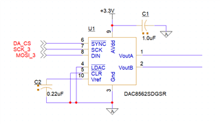
Here's the schematic that we are using:

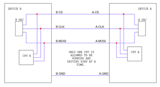
I understand that the SYNC pin is not the same as "chip select", but for our intent that going low means that we are talking to it, and going high means that we are not talking to it, it's close enough.

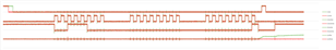
Here's a picture of what we are sending to the chip:

Top yellow: chip select/sync

Green: Clock

Blue: MOSI

Bottom pink: VREF (but scaled up a bit so its easier to see even though its always 0 in this image).

This is the first time after power up that chip select goes low, so nothing else has been talking to it and it should be in a known state.

I would expect that the signals in the picture that were given to that DAC chip would have turned on the VREF. But VREF stays low (even after things have gone to steady state, like multiple seconds after).

Is there something that we are missing? I would love feedback.

---------------------------------------------------------------------------------------------------

Additional info:

  • Software SPI (bit-banging) works. I am able to control the DAC by commanding the pins on and off with the main CPU and not the hardware peripheral built into our microcontroller.
  • We are using the ATSAME54P20A microcontroller. Heres the datasheet
  • We have actually used the DAC8652 before on a older project. Lets call that board "A" and call the new troublesome board that we are working on "B"
  • We have hopefully ruled out PCB layout mistakes
    • most importantly by using a known good "A" board and joining the SPI lines from the "A" board to the "B" board and the "A" board can correctly control the DAC on the "B" board.
      • Let me know if that test makes sense to you or if you want to know more. I have a lot on info on that but dont want to clutter up this post
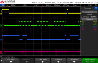
      • The Oscilloscope watched what was being transmitted over these SPI lines without having to disconnect anything (to rule out human error of misplacing things)
      • The traces were "Very Very Very" close, meaning that as far as SPI protocol is concerned, they are identical. I have overlaid them on top of each other, so let me know if you want to see them.
        • they are so close that they are indistinguishable for 90% of it near the ends.
      • I also have csv and excel files of the data from the scope if you are curious and want to analyze it, just ask.
    • by checking and double checking continuity for shorts and breaks
  • We have hopefully ruled out incorrect SPI configuration by using all 4 combinations of CPOL and CPHA
  • We have hopefully ruled out issues with microcontroller configurations by using the same microcontroller as the known good "A" board
  • It "shouldn't" matter but just in case, we also transmitted a "reset" command first to see if that would help. It did not. The command is [0x28 0x00 0x01] on page 38 near the bottom (it is the 7th command from the bottom)
  • Putting the DAC onto a breakout board and connecting to it to the board in development via soldering wires. The "A" board was able to control it, but the "B" board still is unable to vie HW SPI
  • We've tried lightly pulling the LDAC high instead of grounding it. didnt work. But the "A" board is still able to
  • We've tried different SPI speeds. No luck.
  • We've scoped all 10 pins to look for anomalies or differences between the "A" board and the "B" board when communicating to the exact same chip (not the same model, but the exact same piece of silicon and plastic without desoldering it) and they were still identical. We had the scope leads as close as we could get them to the DAC.
  • Hi Andrew, 

    Thanks for the detailed writeup. Your assumptions from the datasheet are all correct. You can directly ground LDAC and CLR. 

    The reference remains powered down while either of the DAC channels are powered down. Have you also written the command to enable one of the DACs and then check the reference? I'm not sure if you're using the exact same sequence on this new board as you are on the "A" board. You mention using the same microcontroller, but you didn't comment on the code running on each. If you are using the same sequence, then I assume this is not the issue. 

    And have you tried using SPI from the "B" board to control the DAC on the "A" board?

    Best,

    Katlynne Jones

  • Thank you for responding.

    Immediately after sending the command to select the VREF, we then send the command to write to DACA and update DACA [0x18, 0x66, 0x66] which should get us roughly 2v. 

    After sending the first command from the "A" board, the VREF on the "A" board and on the "B" board go to 2.5v after a few microseconds.

    then after sending the command to write to and update DACA, the VoutA goes to 2v on both the "A" and "B" boards.

    But if the "B" board sends the commands, then after writing the command to use the internal refrence, VREF stays low, unlike the "A" board transmission.

    And after that if the "B" board sends the command to write to and update the DACA, then the VoutA stays low unlike the "A" board transmission. Also VREF stays low after this too.

    This takes place after powerup and the CS has not gone low at any time before this. Also, we have tried sending the reset command first, but there was no difference, The "A" board could still control "A"s dac and "B"s dac, and "B" board could not control any dac.

    Allow me to explain more on how I know that they are the same signals.

    Heres a schematic of how to boards are connected together:

    <br>

    <br>

    <br>

    <br>

    <br>

    <br>

    CS is connected to CS, CLK to CLK, MOSI to MOSI, and GND to GND.

    And only one CPU is supposed to be running at the same time so that they do not fight over the SPI lines.

    I then took a Oscilloscope and got the CSV data for the transmissions and I was able to overlay them in excel to look for differences.

    I cant upload higher quality images, but here is a link to a spreadsheet with the graph that's off to the right. Also all of the data is in the file too: https://prefutil-my.sharepoint.com/:x:/g/personal/amcclary_preferred-mfg_com/ESkdlQ022ylFlxdOmsPziCoBjlbAYFRTKmdf6tl08i73GA?e=iFFeb9

    Green is the "A" board transmissions. Red is the "B" board transmissions. Orange is where they overlap. The only difference is that the "B" board pulls cs low for longer before clocking. Other than that, they are identical in terms of SPI protocol.

    Let me know if you have a hard time opening it. I made sure to turn on permissions for everybody, but you never know if it goes back.

    So I can say with great certainty that I am sending identical SPI signals to the exact same silicon and plastic chip but get different outcomes.

    Just in case if there is any confusion, it is the exact same chip with no hardware differences. I don't even move the oscilloscope leads because they are both talking to the same chip.

    Also to answer your other question, the "B" board is unable to control the "A" board's DAC. But I have not gone through and made a detailed analysis of the signals on that board. They should be similar, but only differ in terms of small amounts of noise.

    If you disagree with any of my findings or think I came to a wrong conclusion, let me know. I'm prone to logical fallacies just as much as anyone else. And I'd love to figure out what we're doing wrong

  • Also, I'd like to add that the default state for the DACA and DACB registers of the DAC are powered on. (not that you were implying that they weren't, but I just thought it was worth noting). - page 32 Table 5 first row.

  • Hi Andrew, 

    Going back to your original post, you say bit banging works with the main CPU. Is this a different device from the ATSAME54P20A? Or if they are the same device, was this bit banging done with the same SPI pins as the SPI peripheral, or different pins that you wired over? 

    You show grounds being connected from board A to board B in the block diagram, but are you sure there is a good ground shared from CPU B to DAC B? 

    Have you found this issue on multiple 'B' boards that you've manufactured? 

    Best,

    Katlynne Jones

  • Thank you again for helping with this!

    "Is this a different device from the ATSAME54P20A?": Yes, it is the same model of CPU.

    "was this bit banging done with the same SPI pins as the SPI peripheral": I bit banged the SPI protocol using the same CS, MOSI, and CLK pins as would have been used by hardware SPI. The only difference should be that software SPI is a lot slower than the Hardware SPI

    "are you sure there is a good ground shared from CPU B to DAC B": Good question. Let me double check that. The ground connection is very good. Measured with multimeter, and checked with Oscilloscope to look for groundbounce or noise. Seems to be a great connection

    "Have you found this issue on multiple 'B' boards that you've manufactured?" Yes, every "B" board seems to be this way.

  • Hi Andrew, 

    That's good to know that the bit banging method used the same pins on the same CPU. That makes my comments about the hardware connections between CPU B and DAC B less relevant. 

    You mentioned originally that lowering the SPI frequency did not help:

    We've tried different SPI speeds. No luck.

    Did you try as low of a frequency as the bit banging method? 

    Best,

    Katlynne Jones

  • I only tested as low as 200khz HW SPI. Software SPI could only go as fast as 166khz

  • Hi Andrew, 

    Oh, I see, I got it backwards. Your HW SPI was faster than SW SPI. In that case it likely isn't an issue with timing violations with the slower SW SPI. At this point I'm thinking the issue could be with the longer CS delay on the B boards as it's the only thing that is different, and you've seems to have ruled out layout issues by proving the HW SPI works on the B boards. Can you do an experiment with the HW SPI to try to mimic the longer CS delay that is there in SW SPI before the first rising edge of SPI? 

    I'm not finding any data on any maximum timing requirements this device might have, but it's possible that there are. For example, we spec 13ns minimum setup time from the CS falling edge to the first SCLK falling edge. It's possible that there is actual some maximum time that will cause a timeout. We don't purposefully include a SPI timeout in any of our DACs that I'm aware of. If you're able to reproduce the failed communication with HW SPI by increasing the delay between CS and the first clock edge that would indicate to me that this is the issue.

    Best,

    Katlynne 

  • That sounds like a good test. I'll try it out, maybe tomorrow.

    I think I should be able to add some NOPs in there to increase the delay.

    We have discovered undocumented debug and testing modes by accident in the past with other devices. I wonder if this is something similar.

  • Elongating the delay between the CS and first clock edge did not have any difference.

    Also, we ran some other tests, and with a different brand DAC chip (with the same pinout) it worked fine.

    I'm not gonna say what chip it was because I don't think it belongs here. This is a TI forum, and it just doesn't feel right to point people to other companies.

  • Hi Andrew, 

    I took a closer look at your scope data and there are still only minor differences as far as any timing differences beyond the CS falling edge. I don't think those are contributing factors. I noticed that the working SPI has much larger noise spikes, about +/-1V from VDD and ground. Ignoring that because this is the working board, it also looks like the overall logic level reaches a higher voltage. Are you measuring the SPI signals near the DAC or near the MCU? Is there a chance that the SPI signals reaching the DAC are being attenuated? Maybe not likely considering you had the bit-banging SPI working on those same pins, but I'm low on ideas for other things to check out. 

    Best,

    Katlynne Jones

  • Thanks for your continued assistance!

    The measurements were taken as close to the DAC as we can reliably get, but not touching the pins directly.

    .

    .

    Also, on a good note! I was experimenting and I noticed that hooking up oscilloscope leads changed the behavior of different brands of DAC chips. From there, I was able to find the sweet spot of capacitance that made the TI DAC work. The signals still look the same, but now the TI DAC works!

    I suppose that there must have been noise at a frequency higher than what my scope could read.

    So I guess that is my conclusion right now, there must have been some really high frequency noise that the scope could not pick up, which is why the signals looked the same.

    I guess I can call this solved now, thanks for looking into it!

  • Hi Andrew, 

    Great to hear you were able to get it working. Let me know if you run into any other issues. 

    Best,

    Katlynne