


Other Parts Discussed in Thread: ADS1298, ADS1296
A time ago I designed the next PCB 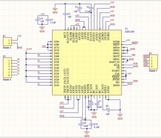 in order to test the ADS1298, it worked well as I expected but there was a problem, the voltage reference generated was nos appropriate for my purposes so I designed a new PCB which implements an adequate voltage reference to use as a virtual ground for the input signals as shown here
I have been testing this new PCB with the same configurations and connections for SPI communications than the first PCB I mentioned, but output data at DOUT appears to be 0 without changes, I have checked connections on PCB and everything looks fine, I would appreciate if someone tells me the problem on this design or something I am missing.
If someone has an schematic to illustrate the appropriate way to test the ADS1298 that would be great.
Regards,
Rashid

