


Tool/software:
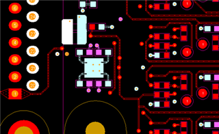
The ADS1204 voltage sampling circuit used was damaged, and two ADS1204 pieces were damaged on one board. The PCB photo is shown in Figure 1.
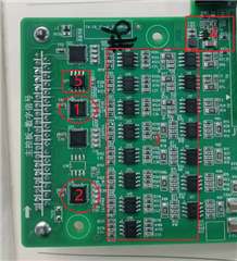
The parts in Figure 1 are divided into:
1: Damaged ADS1204, the preliminary test of this CHA+ port is damaged, the ground resistance is 0.8Ω;
2: Damaged ADS1204, the initial test found that the REFOUT port is damaged, the ground impedance is 0.8Ω, an input port CHB+ is damaged, the ground impedance is 0.8Ω;
4. 5V power supply for AVDD, BVDD uses another 5V power supply, AGND and BGND are connected through a magnetic bead.
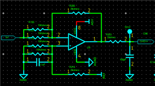
5. REF voltage follower operation amplifier.
6. ADS1204 input conditioning op amp, this part of the op amp uses 5V power supply, use ADS1204 REF voltage follower offset. The peripheral circuit screenshot is shown in the following figure.
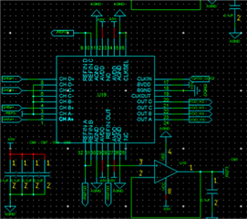


the layout of ADS1204
Additional information:
CLK uses a 20MHz clock with an external FPGA
Could you kindly give some advise,thanks
