This thread has been locked.

If you have a related question, please click the "Ask a related question" button in the top right corner. The newly created question will be automatically linked to this question.

ADS1278EVM-PDK: Power-Up Issues with Old ADS1278 EVM (standalone using FPGA)

Part Number: ADS1278EVM-PDK
Other Parts Discussed in Thread: ADS1278

Tool/software:

Hello everyone,

We are using an older ads1278 EVM to prototype our system and have set up the power supply as follows:

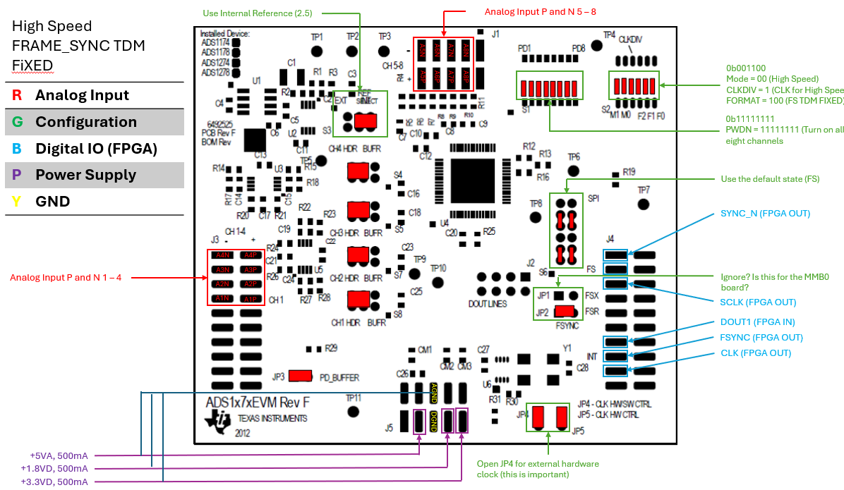
  • Power Sources: Two separate dual-channel DC power supplies providing 5V, 3.3V, and 1.8V, each set to 0.5A limit
  • Issue: The board does not power on standalone (unable to receive ADC data using an FPGA system that worked the lastest ads1278 EVM).
  • Current Observation: When all three power supplies were turned on, the 5V and 3.3V channels drew only ~0.01A, and the 1.8 channel drew no current.
  • ADS1278EVM-PDK Evaluation Module V1.pdf

I have a few questions regarding proper power-up:

  1. Does this EVM have a Power Good indicator or test point to check the status of the power rails?
  2. Is there a required power-up sequence for 5V, 3.3V, and 1.8V?
  3. I connected the grounds of all three power supplies together and tied them to AGND on J5 Pin 6 (top row, middle). Is this the correct approach?

Any guidance on these issues would be greatly appreciated.

Thank you!

  • Hello Yuchen,

    There is no power good indicator on this board.  However, you should verify that the correct voltages are present near the IC pins. 

    Verify AVDD on C41 (should be 5V)

    Verify DVDD on C43 (should be 1.8V)

    Verify IOVDD on C46 (should be 3.3V)

    There is no power-up sequence required for proper operation of the ADC.  However, the /SYNC pin should be toggled after power-up of the board.

    If I recall correctly, the DGND and AGND are not connected together on the board; they were connected together on the MMB0 board.  Since you are using this board without the MMB0 data capture board, you need to short these two grounds together, pin 5 to pin 6 on J5.

    Additional suggestions:

    Verify there is an active clock (typical 27MHz) on R16.

    Verify the device is actually powered up by checking for 3.3V (IOVDD0 on any of the pull-up resistors R32 (both sides).  I have seen a few of these boards where the switch is installed backwards and the position to enable the channels is opposite the user's guide.

    Regards,
    Keith Nicholas
    Precision ADC Applications