Tool/software:
Hello everyone! I’m working on a project using two ADS1235 ADCs (specifically, the ADS1235QWRHMRQ) to monitor the deformation of steel objects using strain gauges. Despite following a straightforward design approach, significant measurement inconsistencies persist, and I’m seeking help to pinpoint the root cause.
Project and Application Context
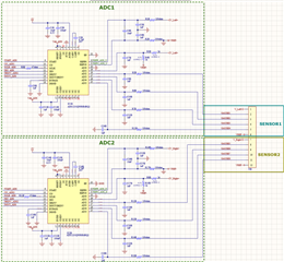
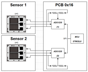
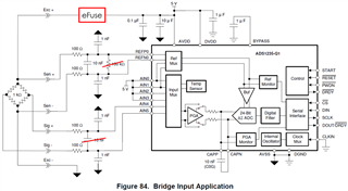
The system is designed to monitor deformation in two steel objects located at different parts of a machine. Each steel object is instrumented with four strain gauges (configured as half Wheatstone bridges), totaling eight strain gauges. The gauges (nominal resistance of 350 Ω, approximately 700 Ω in half-bridge configuration) are measured against a PCB-mounted voltage divider (comprising two 1kΩ resistors) that acts as a reference.
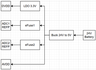
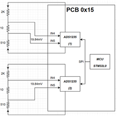
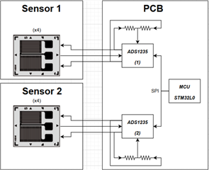
Here is a block diagram of our device:
Hardware and Software Details
PCB Details:
- The design is implemented on a 4-layer PCB, with a dedicated ground layer directly under the ADS1235.
- There aren’t any high-speed signals near the ADS1235 (only the microcontroller clock, which is located far away).
ADC Configuration:
- Model: ADS1235QWRHMRQ
- Settings:
- PGA Gain: 128
- Chop Mode: Enabled
- Filter: Sinc4
- Sampling Rate: 1200 samples per second (sps)
- Delay: 0 µs
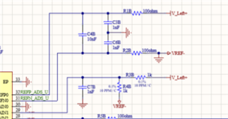
- Additional Hardware: A low-pass filter is used on each channel, formed by a 100 Ω resistor in parallel with a 1 nF capacitor.
Power Supply Details:
- DVDD: 3.3 V
- AVDD: 5 V
- The board is powered by a 24V battery through a buck converter. Although the buck converter’s output voltage shows some variation with changes in the input voltage, its effect on the ADC readings is minimal due to differential measurement.
Issue Description
Expected Behavior:
The ADC should provide stable readings that primarily reflect the deformation of the strain gauges, with minimal noise, drift, or step changes.
Observed Behavior:
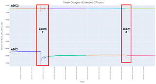
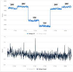
When we installed the system in a machine, we noted inconsistencies on the measurements. For example:
- Step Changes: Sudden jumps in the ADC measurements—see images.
- Drift: Noticeable positive or negative drifts over time (e.g., approximately 20000 ADC levels over a 4-hour period).
Troubleshooting and Testing So Far
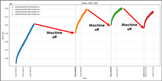
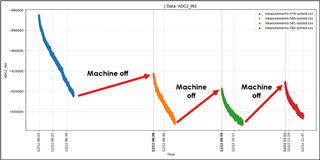
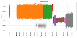
Mechanical Isolation
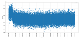
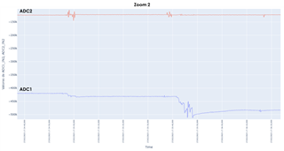
To rule out mechanical influences, the device was placed in the machine without soldering the sensors to any structure. The results still showed steep drifts (positive or negative) and changes upon power cycling:
Power Supply Assessment
We did some tests in our laboratory to isolate identifying if there is an issue with the power supply.Varying the input voltage revealed that while the buck converter’s 5V output does vary with input voltage, the ADC readings remain largely unaffected.
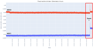
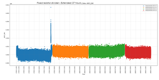
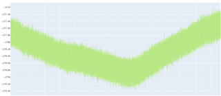
Extended Lab Testing
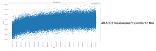
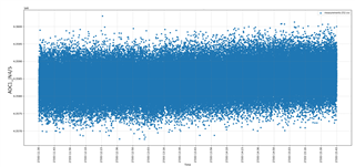
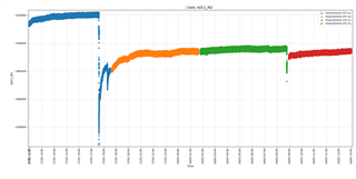
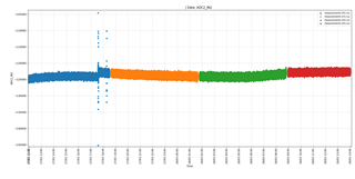
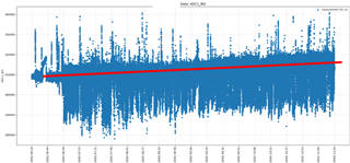
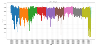
We performed a long test on the lab to check how our device behaves in a controlled environment (temperature and power supply). This is the result of different ADCs:

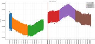
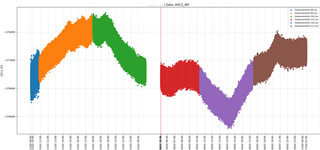
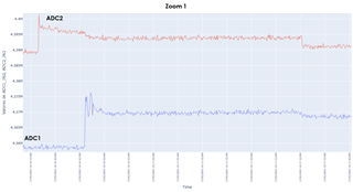
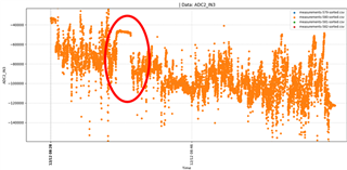
This is a close up on the purple zone (time duration around 4:30hr). Seems there are 600 ADC levels of noise and a drift of 1000 levels in 2 hours:
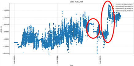
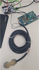
Testing with the ADS1235 Evaluation Board
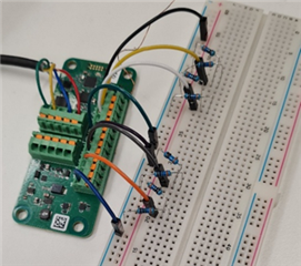
I measured the gauges with the evaluation board, to check if it’s a problem with the PCB that we designed or with the sensors. This is a photo of the setup:
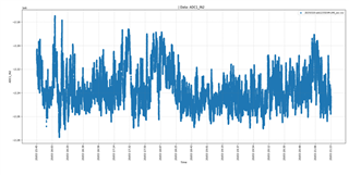
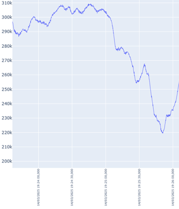
This is the result together with a zoom in on a 2-minute window. It seems there are variations of around 100K ADC levels:
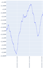
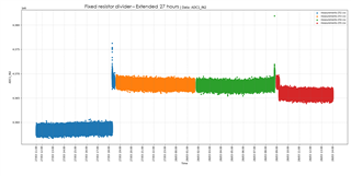
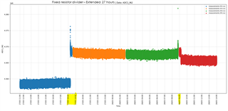
PCB measurements with commercially available resistors
A Wheatstone bridge built with standard resistors was tested to separate the PCB performance from that of the strain gauges. This is a photo of the setup:
This is the result together with a zoom in on a 2-minute window. It seems there are variations of around 100K ADC levels:
Request for Assistance
I’m at an impasse. My testing has not isolated whether the inconsistencies come from:
- A design issue on the PCB (routing, filtering, or layout),
- The strain gauges themselves, or
- An issue with the ADS1235.
Thank you in advance for your insights and recommendations. I’m eager to understand the underlying cause of these issues and would appreciate any guidance or suggestions on further diagnostic steps, potential design improvements, or known issues with the ADS1235 that might explain these behaviors.
Best regards,
Edgar