This thread has been locked.

If you have a related question, please click the "Ask a related question" button in the top right corner. The newly created question will be automatically linked to this question.

ADS7138-Q1: Abnormal read register value, unable to successfully write register

Part Number: ADS7138-Q1

Tool/software:

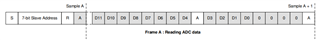
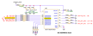
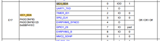
Our team's development board plans to use the ADS7138QRTERQ1 chip as the AD chip to recognize the AD value of the physical keypad (pin KEY_KEY), and transmit the converted AD value to the main control chip AM62A74UMHAAMBR through SOC_SDA and SOC_S2C1_SCL.

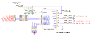
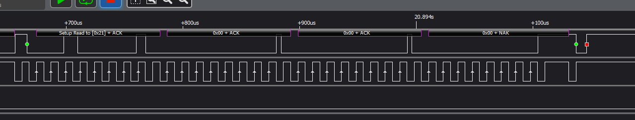
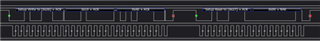
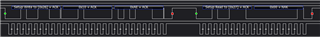
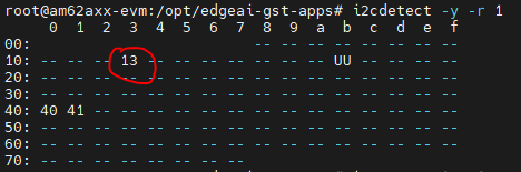
Currently, AD chip devices can be recognized on the I2C bus

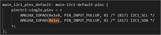
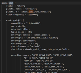
The device tree configuration is as follows:

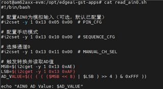
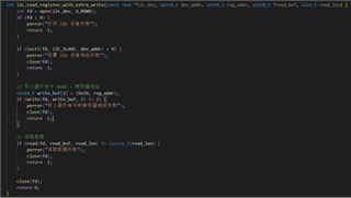
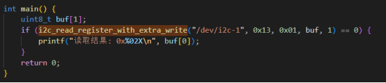
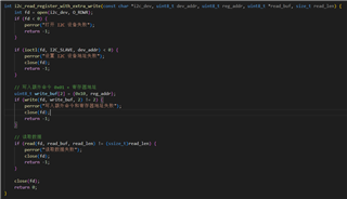
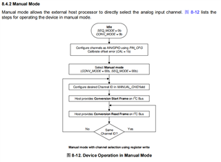
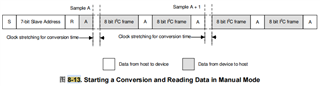
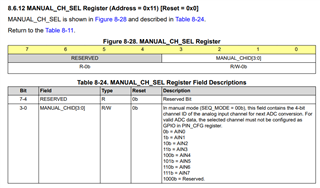
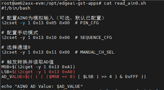
The script content for reading AIN0 is as follows:

The current issue is:

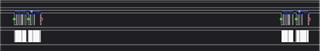
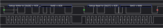
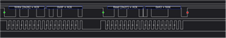
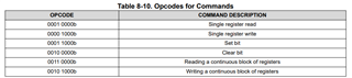
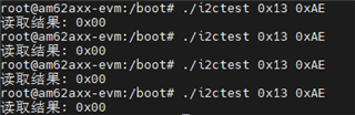
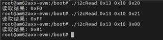
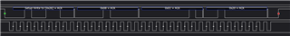
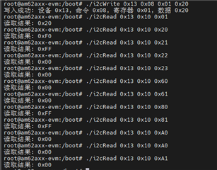
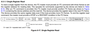
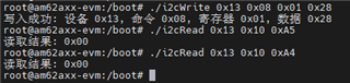
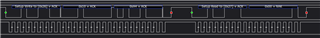
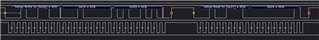
1. Directly read any register using the i2cget - y 1 0x13 command, and the value will be 0xff.

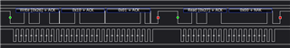
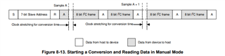
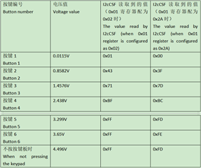
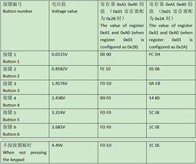
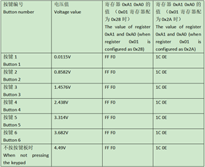
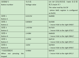
2. When the physical button is pressed, any register is read, and the value read is consistent with the voltage value measured by the multimeter, which can be understood as the AD value.

Why do all registers behave the same?

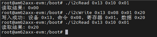
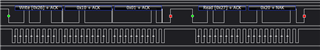
3. When I tried to change the value of one of the registers with a write command and then read the register, I found that the write command did not take effect and it was still 0xff.

Please help me analyze the causes of the problem and provide solutions based on the information above. Thank you.
If there are reference routines provided, that would be even better.

  • Hi Ziming Yi,

    Rather than sending the i2cset utility commands, can you send me a logic capture of the I2C lines?

    Regards,
    Joel

  • Hi Joel Meraz,

    Because we need to collect the AD value of AIN0, I have configured the following registers based on the data manual of the chip and my own understanding:
    1. Configure the PIN_CFG register to ensure that AIN0 is an analog input.
    2. Configure the SEQUENCE_CFG register and select manual mode.
    3. Set the MANUAL_CHSEL register to 0x00 (channel 0).
    4. Trigger conversion (possibly by writing specific registers or sending I2C commands).
    5. Read the Recent-CH0_SB (current data register being captured) and Recent-CH0-MSB registers to obtain a 12 bit AD value.
    But I am not sure if the configuration has been completed correctly, so I would like to ask for your help to confirm if there are any issues with the process of configuring registers in order to fulfill the requirement of reading AD values?

    Regards,

    Ziming Yi

  • Hi Ziming,

    It seems like the order you described is correct, but I need to verify that the utility is sending the correct data to the device as you expect it to. A logic capture or an oscilloscope capture of your sequence should suffice. I have observed in the past that these I2C command line utilities don't send data as expected.

    Regards,
    Joel

  • Hi Joel Meraz,

    So, is there anything I can provide to help you further validate the analysis?

    Regards,

    Ziming Yi

  • Hi Ziming,

    Yes, a logic capture probing the SDA and SCL pins of the ADC will help. Below is an example, with the SDA line on top and the SCL line on the bottom.

    Alternatively, you can provide an oscilloscope capture of the SDA and SCL lines, but this is much harder to read and decode. If you do have a logic analyzer available, I would much prefer that.

    Regards,
    Joel

  • Hi Joel Meraz,

    This is the content of the read_ain0.sh

    I used a logic analyzer to capture the IIC waveform when calling the read_ain0.sh as follows:


    1、 When the physical button is not pressed, the result of calling the read_ain0.sh is as follows


    The waveform captured by the logic analyzer is as follows:


    This is the detailed signal of the waveform on the left


    This is the detailed signal of the waveform on the right


    2、 When holding down the physical button, the result of calling the read_ain0.sh is as follows


    The waveform captured by the logic analyzer is as follows:


    This is the detailed signal of the waveform on the left


    This is the detailed signal of the waveform on the right


    If there is any other information that needs to be supplemented, please contact me
    Thank you for your help

  • [deleted]
  • Upon further review, the controller seems to be sending the right 7-bit address, but the logic analyzer is parsing it incorrectly. The 0xAE command still seems to be incorrect however. To start, consult the ADS7138-Q1 "Programming" section (section 8.5). Here, every command opcode goes as such:

    A 7-bit address is provided, followed by a R/~W bit, and a device ACK. The following 8 bits are opcodes for different device register access functions. See the table below for options.


    Right now, it seems like the read bit is sent after the 7-bit device address, and the register address is provided immediately after. However, an opcode needs to be provided before the register address is provided. Below is the command structure for a single register read. I believe replacing the register address with the opcode and replacing register data for the register address might help, but this is more of a concern with the command line utility in use which I have no insight on.

    Regards,
    Joel

  • Hi Joel Meraz,

    We wrote a code based on the data format read from a single register

    So now, regardless of whether the physical button is pressed or not, the value read is 0x00

    This is the data captured by the logic analyzer

    Regards,

    Ziming Yi

  • Hi Ziming,

    Can you reattach the logic capture? It is a little low resolution, and I can't quite make out the numbers.

    Regards,
    Joel

  • Hi Joel Meraz,


    This is the data captured by the logic analyzer

    And this is the key code content

    So now, regardless of whether the physical button is pressed or not, the value read is 0x00

    Regards,

    Ziming Yi

  • Hi Ziming,

    This sequence looks correct. The reason that the RECENT_CH7_LSB register is not updating is because the STATS_EN bit in the GENERAL_CFG register has to be enabled first for the statistics registers to store the latest values.

    Regards.
    Joel

  • Hi Joel Meraz,

    Summarize the current situation:

    Currently, the operation of reading I2C registers is verified to be able to successfully read the value of a single register. I read many registers with default values other than 0x00 according to the chip manual, and the results were all correct.

    In addition, the operation of writing I2C registers and verifying can also successfully change the value of a single register. Just as writing the value 0x02 to the 0x01 register, the verification code before and after writing is valid and successful.

    Taking the 0x01 register as an example, the data captured by the logic analyzer for reading/writing registers currently conforms to the format specified in the chip specification.

    Read 0x01 register

    Write 0x20 to the 0x01 register

    Read 0x01 register again

    However, when pressing the physical button, reading 0xA0 will still be 0x00.

    I also read all the registers related to CH0 once. The results read when pressing the physical button do not look like AD values.

    So I would like to inquire:
    1. Are there any registers that need to be configured to enable the AD chip to process and convert analog signal inputs?
    2. Which register is being read to read the AD value of AIN0 input? Is it Recent_C0_LSB and Recent_C1_LSB or other registers?

    Regards,

    Ziming Yi

  • Hi Ziming,

    ADC conversion data can be read in two ways:

    1. Initiating a read to the device (Figure 8-13)

    2. Reading from the  RECENT_CHx_LSB and RECENT_CHx_MSB registers. This requires first setting the STATS_EN bit to 1 to enable updating the registers. You also need to set the CNVST bit to 1 if you will only be using register accesses to convert. A single register read is described below.

    So at the moment, it seems like setting the CNVST bit in the GENERAL_CFG register is still missing. The device has not initiated any conversion at the time of reading back from the registers, so there is no conversion result.

    Regards,
    Joel

  • Hi Joel Meraz,

    Today, I tried two ways to read AD values based on the reply
    Method 1: Start reading the device (Figure 8-12)

    According to the process, the configuration is known, but since many registers have default values that meet the configuration requirements, it is only necessary to first read and confirm whether the relevant registers have default values. If it is the default value, it meets the configuration requirements and only requires CAL=1 to be configured. Then send S+7-bit device address+read flag+A

    Verification process

    The host provides the following values for the Conversation Start Frame read on the bus:

    Assign the LED lights from left to right to the 6 physical buttons numbered 1-6

    My question regarding this verification method is:
    1. May I ask if the verification process above complies with Device Operation in Manual Mode
    2. If yes, does the value read by i2cCSF represent AD value? Why doesn't it correspond well with the measured voltage?


    Method 2: Read from the Recent-CH0_SB and Recent-CH0.MSB registers.
    Need to set the STAT3 and CNVST bits to 1

    Then I saw the description in the 0x01 register and thought CAL might need to be set to 1. So I separately verified that STAT3=1 CNVST=1、CAL=0, And the results of STAT3=1, CNVST=1, CAL=1.

    The values read in the morning are as follows:
    Unfortunately, I didn't take a screenshot of the data captured by the logic analyzer
    Number the keypad 1-6 from left to right using LED lights

    However, in the afternoon when I was preparing to reply, I read the following values:
    Number the keypad 1-6 from left to right using LED lights

    Now I don't know where the problem lies.
    1. Not sure if the value read in the morning is the correct AD value?
    2. Why can I read the value in the morning, but later in the afternoon I can only read 1C 0E

    Regards,

    Ziming Yi

  • Hi Ziming,

    It appear that the controller is sending the NAK to the device in the logic capture frames you provided. It only is expecting one 8-bit data frame from the device, and a NAK tells the device to stop outputting conversion data. Because of this, you are not reading in the full conversion. You will need to configure the controller to read in more than 1 byte before sending a NAK, but I don't know how to accomplish this with your specific command line tool.

    1. Due to the condition above where the controller sends a premature NAK, I will say that this sequence is not meeting the requirements, and you will need to change the controller configuration as mentioned to read in at least 2 bytes of data at a time, as 1 ADC conversion is encoded across 2 bytes. 

    2. At the moment, no. The full 12-bit conversion is encoded across 2-bytes. The first byte contains the first 8 bits of ADC data (D[11:4]), and the next byte contains D[3:0], followed by 4 zeroes at the end by default.

    I do believe we are getting closer to the desired result, and the logic captures are very helpful in debugging this. Please continue sending logic captures, and I can help further.

    Regards,
    Joel

  • Hi Joel Meraz,

    Good news!!


    After configuring the registers according to the MANUAL MODE process, I directly set the 01 register to 0x2A,
    I modified the code for the startup frame and sent it in the following format:


    Start signal+7-bit device address (0x13)+1-bit read flag bit (1)+ACK+2 bytes of ADC data


    The values read are as follows:


    It seems that the value read is the AD value.

    And as mentioned earlier, in Method 2, I also successfully read the value of RECENT_C0_SB/MSB, which matches the AD value

    So the current reading of the AD value from the AIN0 channel has been successfully completed. Thank you very much for your guidance and assistance.

    But then I encountered a new problem, and I will provide a detailed explanation of the situation in the next post

    Regards,

    Ziming Yi

  • Hi Joel Meraz,

    As shown in the hardware schematic diagram

    The AD value of the photoresistor is input through the AIN2 channel.

    So I tried to read the values of Recent_C_2LSB and Recent_C_2MSB to check if they match the measured voltage values.


    However, the read register result is 00

    So I would like to ask if there are any other configurations that need to be done?

    Regards,

    Ziming Yi

  • Hi Ziming,

    First of all, I'm glad your first issue was fixed! 

    I believe the reason for this is that Channel 0 is still selected. To change to Channel 2, you must configure the MANUAL_CHID field in the MANUAL_CH_SEL register (address 0x11). After selecting the channel, you can then start the conversion with the CNVVST bit and read from the RECENT_CH2 registers when the conversion is complete.

    Let me know if this helps or if I can provide more detail. The general process is described in figure 8-12, but instead you are manually initiating conversions with the CNVST bit and reading the conversions from the RECENT_CHx registers.

    Regards,
    Joel

  • Hi Joel Meraz,

    It seems successful bro. Thank you very much for your guidance and assistance during this period. Once again, I would like to express my gratitude.

    If there are any related issues encountered in the subsequent development, I hope to have the opportunity to continue discussing with you under this post.

    Regards,

    Ziming Yi

  • No problem! Glad to be of help. Feel free to reach out if anything else arises.

    Regards,
    Joel