Tool/software:
Hi,
I am working with the ADS5560 and I have concerns about the input clock signal when operating in single-ended mode with AC coupling (CLKM grounded through a 0.1 µF capacitor).
Issue:
-
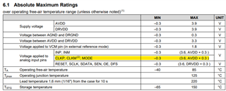
According to the datasheet, the absolute minimum voltage for CLKP is -0.3V.
-
Since my clock signal is AC-coupled, it is centered around 0V, meaning that it inevitably crosses the -0.3V limit.
-
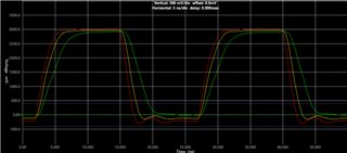
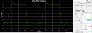
I simulated the received signal using HyperLynx, and it looks like this:
As you can see, it crosses the -0.3V limit.
Analysis:
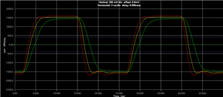
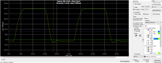
I assume that the -0.3V limit accounts for the internal 5kΩ pull-up resistor to VCM = 1.5V. So, I repeated the simulation, now including the effect of this pull-up resistor:
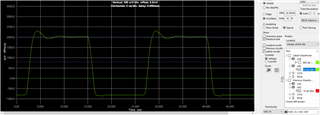
As expected, the signal is now centered around 1.5V, but it still violates the -0.3V limit. To keep the signal within the specified range, I found that I need a minimum series resistor of 250Ω:
However, adding such a large series resistor degrades the slew rate, which in turn increases jitter, potentially affecting ADC performance.
Questions:
-
How strict is the -0.3V limit on CLKP? Given that AC coupling inherently results in voltage excursions beyond this limit, is this specification meant to be an absolute restriction?
-
Is there a recommended way to AC-couple the clock signal while staying within the voltage limits without degrading slew rate?
-
Regarding Figure 53 of the datasheet, I tested connecting and disconnecting VCM to CLKM as suggested, but I noticed little to no difference (since CLKM already has an internal 5kΩ pull-up to VCM). Is there any practical benefit in connecting VCM externally to CLKM?
Any insights would be greatly appreciated.
Thanks!