Other Parts Discussed in Thread: DAC8832, TIPD192, THS4561, PSIEVM, , DAC82001
Tool/software:
Dear TI experts:
We try to use DAC8831 to generate analog signals, but the output signal of DAC8831 is noisy. Could you help us analyze the reasons and improve the quality of the DAC8831's output signal?
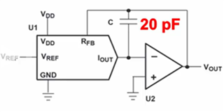
DAC8831 evaluation board 1
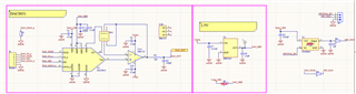
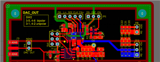
The evaluation board is designed based on TIPD192. We use DAC8831 (SO-14) to replace DAC8832 in TIPD192. The schematic and PCB are as follows.
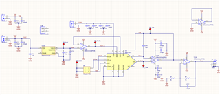
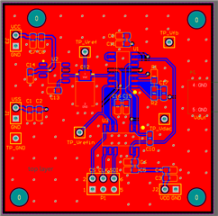
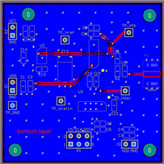
Fig.1 to Fig.3 are the schematic and PCB of the DAC8831 evaluation board 1.
The test setup is as follows.
The single end signal is input to a single-end-to-differential circuit (THS4561), the differential signal is sampled by ADS9120EVM (bought from TI). The data acquisition part (the single-end-to-differential circuit and ADS9120EVM) is verified by PSIEVM (bought from TI). The THD of the data acquisition part is as low as -118 dB.
The FPGA control board is also verified in other experiment. It is used to control the sampling of an ADC. The sampled sine wave is clean.
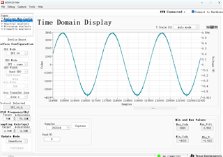
We use the DAC8831 evaluation board 1 to generate a single-end sine wave signal, and use the same data acquisition part to sample the sine wave signal. The experiment shows that, the output signal of DAC8831 is impure.
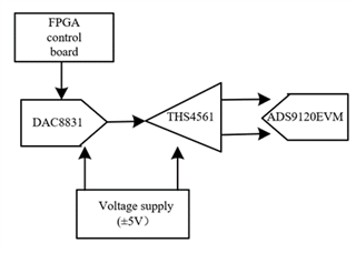
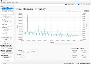
Fig.4. Test setup.
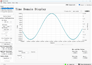
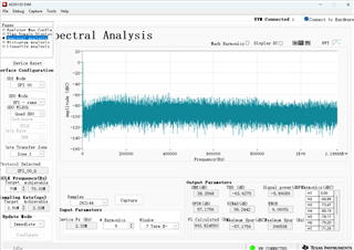
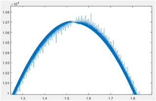
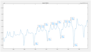
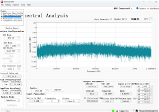
Fig.5 and Fig.6. The sinusoidal waveform and spectrum of the DAC8831 output (board1).
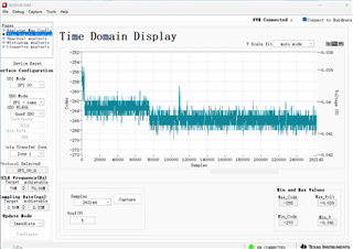
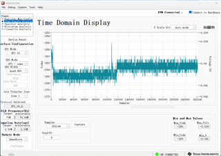
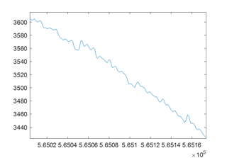
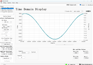
Fig.7 and Fig.8.The digital waveform of the DAC8831 is set to be DC (voltage = 0V). The output results are as above.
DAC8831 evaluation board 2.
We also design another DAC8831 evaluation board based on DAC8831EVM. In this board, analog ground and digital ground are separated, and connected by a magnetic bead on the bottom layer.
The output of DAC8831 is also bad.
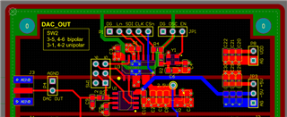
Red(1)-top layer, green(2)-ground, dark red(3)-power, blue(4)-bottom layer. The oscillator and its nearby resistors and capacitors are not placed (DNP).
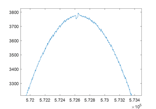
The sinusoidal waveform and spectrum of the DAC8831 output (board2).