This thread has been locked.

If you have a related question, please click the "Ask a related question" button in the top right corner. The newly created question will be automatically linked to this question.

AFE11612-SEP: Queries Regarding ADC Reference, ENOB, AVcc, and Remote Temperature Inputs

Part Number: AFE11612-SEP

Tool/software:

Hello,

I have a few technical queries regarding the usage of your ADC device:

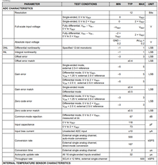
  1. Are the error values mentioned in the datasheet (such as INL, DNL, and offset) characterized using the internal or external voltage reference?

  2. What would be the expected ENOB when using:

    • The internal reference, and

    • An external 2.5V ±0.05% reference?

  3. If I do not plan to use the DAC functionality, can I leave the AVcc pin floating, or does it need to be tied to a specific potential?

  4. The device includes two remote temperature sensing channels. Is it possible to use them as general-purpose differential ADC inputs? Additionally, can they be used for interfacing a thermocouple?

  • Hi Dhir,

    1. These specs are using the internal reference.

    2. ENOB: I will look into this

    3. You should tie AVCC to AVDD. The AFE will not power on if AVCC is not powered.

    4. Thermocouple: I will look into this as well.

    I'm out of office currently. I will be back in next week and I'll get the answers to your remaining questions.

    Thanks,
    Erin

  • Hi Erin,

    Thank you again for your support.

    I have a few additional questions:

    1. What level of accuracy or error can I expect when using an external 2.5V ±0.05% voltage reference?

    2. What are the typical gain error and zero code error when using the internal reference?

    3. I would also like to understand the power supply sequencing requirements. My planned configuration is as follows:

      • AVDD = DVDD = AVCC = 5V

      • IOVDD = 3.3V

      • VREF = 2.5V

      Does the sequencing of these supplies matter? If yes, could you recommend a way to minimize the number of power supplies needed? I’d prefer not to use four separate regulators if it can be avoided.

    Additionally, if I am not using the DAC functionality, can I leave the DAC output pins floating?

    Looking forward to your guidance.

  • Hi Dhir,

    1. You can estimate TUE (total unadjusted error) by taking the root-of-summed-squares of the error sources together.  You will need to convert to common units, like %FSR.  So, for example:

    ADC TUE(%) = sqrt(OSE^2 +GE^2 + INL^2 + REFERR^2)

    where OSE is offset error, GE is gain error, INL is INL, and REFERR is your reference error.  This is a good way to estimate when TUE was not measured directly on the device.  Note that INL is pretty much reference independent, but GE is increased with reference error.  

    2. OSE will not change really with a different reference voltage, but you could expect GE to be additive with reference error.

    3. I will let Erin comment here. 

    4. Unused DACs can be left floating.

    Thanks,

    Paul

  • Hello Paul,
    Thanks for sharing.

    Could you please let me know how can I terminate unused DACs? I don't want to leave them floating. Also, I am hoping that you can also help me with below questions:

    1. The device includes two remote temperature sensing channels. Is it possible to use them as general-purpose differential ADC inputs? Additionally, can they be used for interfacing a thermocouple?

    2. I would also like to understand the power supply sequencing requirements. My planned configuration is as follows:

      • AVDD = DVDD = AVCC = 5V

      • IOVDD = 3.3V

      • VREF = 2.5V

      Does the sequencing of these supplies matter? If yes, could you recommend a way to minimize the number of power supplies needed? I’d prefer not to use four separate regulators if it can be avoided.

    3. I am planning to calibrate the ADC. Could you please confirm whether the error characteristics are the same across all channels, or if each channel needs to be calibrated individually?
      Additionally, if I’m using two separate ADC ICs, would each IC require individual calibration?

    Regards,
    Dhir

  • Hi Dhir,

    There should be no issue with leaving the DACs floating, especially if you do not intend to use them. By default, the DACs are in a power off condition. If you want to terminate these outputs, then a 10k resistor to ground would be a safe way to do so. 

    1. The temperature sensing channels only work with diodes as far as I can tell, not thermocouples. They also cannot be used as general ADC inputs.

    2. There is a "preferred" order in the datasheet of IOVDD, DVDD/AVDD, then AVCC. It's fine if DVDD, AVDD, and AVCC go on at the same time, and they can use the same power supply. IOVDD doesn't necessarily have to come on first, but it is preferred. VREF is fine coming on at the end of the sequence.

    3. Each channel uses the same ADC, but goes through a MUX. There may be slight offset error or gain error differences between each channel, but overall each channel should be nearly the same. I recommend calibrating each IC, as the ADCs will have different characteristics.

    Thanks,
    Erin

  • Hi Erin,

    Thanks for the clarification.

    Regarding the power on sequence, I plan to use the internal 2.5V reference. Could you please elaborate why is the power sequence preferred and what sort of issues can occur if power sequence isn't followed?

    Also, could you please help me with another query I had regarding the TMS570 MCU in another post?

  • Hi Dhir,

    I don't recall exactly what could happen if they are not sequenced correctly. If a customer wants to do an unpreferred sequence, we generally recommend doing a device reset (either through the RESET pin or by writing to the RESET register). I haven't had anyone come back with issues when using a reset.

    I also helped out with the TMS question. I left it open in case the microcontroller team has anything they want to add, not sure why they haven't gotten to the question yet.

    Thanks,
    Erin

  • Thanks, Erin!

  • Hello Erin,

    Could you please clarify whether the sink and source current values are specified per I/O pin or for all I/O pins combined? I’m trying to determine the maximum current consumption on the IOVcc rail at 3.3V.

    While I understand that a reset might help mitigate issues arising from an incorrect power-on sequence, I would like to better understand the implications:

    1. What are the potential risks or malfunctions that could occur if the recommended power-on sequence is not followed?

    2. Does using a non-preferred sequence introduce any additional electrical or thermal stress on the component over time?

  • Hi Dhir,

    These are per I/O pin. 

    I'll talk with a designer about the sequencing issue since the datasheet doesn't specify what could happen. They may be able to run simulations to give a better idea.

    Thanks,
    Erin

  • Hi Dhir,

    Simulations would take a while to run, but the designer said in general you could expect to see higher current on VDD/VCC due to ESD diodes not being supplied properly, and memory not loading properly. If the time period is short the electrical damage should be nothing; note that we don't have any data on long term stress with non-ideal sequencing. The memory issue is fixed with a hardware/software reset, which is what we generally recommend. Let me know if you have any other questions!

    Thanks,
    Erin

  • Thanks, Erin!

  • Hello Erin,
    Any update on the simulations? Also, I plan to use three ADCs in a single system and intend to use the VREF output of one ADC as the VREF input for the other two. Please provide any relevant application notes and the recommended decoupling capacitors for this configuration.

  • Hi Dhir,

    No update yet, unfortunately. You can use a combination of these two figures for the capacitance. According to the datasheet:

    Put a 100pF to 10nF capacitor on the REF-OUT pin.
    For the device using the internal reference, put a 4.7uF on the REF-IN/CMP pin.
    For the other two devices, put a small capacitor (100pF - 10nF) on the REF-IN/CMP pin. The external reference will go in at this pin.

    Thanks,
    Erin

  • Thanks Erin! Also, requesting you to please share the simulation results asap.

  • Hi Dhir,

    Apologies for the delay! It is apparently extremely difficult for the designer to do a long period simulation for this, but for short term simulations he saw nothing going badly. I've set up an EVM to run with only VIO on over the weekend to see if there's any issues when I come back on Monday. From the few minutes of setup, I did not see any high currents or VDD/VCC voltages being pulled up. 

    Thanks,
    Erin

  • Hi Erin,

    Thanks for sharing. Eagerly waiting for the test results.

  • Hi Dhir,

    Device still functions well! I don't think there should be any issues with doing an incorrect sequencing over time. Just make sure to do a software reset after you power up so prevent any device memory loading issues.

    Thanks,
    Erin

  • Thanks Erin!