This thread has been locked.

If you have a related question, please click the "Ask a related question" button in the top right corner. The newly created question will be automatically linked to this question.

DAC8565EVM: DAC CONNECTON ISSUE

Part Number: DAC8565EVM
Other Parts Discussed in Thread: DAC8565

Tool/software:

Hello TI Team,

I am currently working on interfacing the DAC8565 with an ESP32, but I am not observing any output at the expected pin (JMP9 - Out A). Below are the details of my setup, connections, and code:

Connections:

  • MOSI (ESP32) → DIN (DAC)

  • CS (ESP32) → SYNC (DAC)

  • SCLK (ESP32) → SCLK (DAC)

  • AVDD → 5V

  • IOVDD → 3.3V

  • LDAC, VREFL → GND

  • ENABLE → Left as default (not actively driven)

  • RST → Setting as High in the code.

We are measuring the output at JMP9 (OUT A).

I have attached the following for your reference:

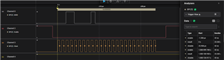
  • The SPI timing diagram captured during communication

  • The Arduino code used for communication, using SPI MODE2.

Despite this setup, there is no output observed from the DAC. I would appreciate your guidance on what could be going wrong or what I might be missing.
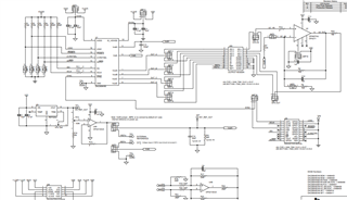
#include <SPI.h>

// Pin mapping
#define DAC_CS     5   // SYNC
#define DAC_RST    18  // RST
#define SPI_MOSI   19
#define SPI_SCLK   23

void sendDAC8565(uint8_t cmd, uint8_t addr, uint16_t value) {

  // Build the 24-bit frame
  uint8_t firstByte  = (cmd << 4) | (addr & 0x0F);
  uint8_t secondByte = (value >> 8) & 0xFF;
  uint8_t thirdByte  = value & 0xFF;
  

  digitalWrite(DAC_CS, LOW);     // SYNC low to start

  uint8_t data[]={firstByte,secondByte,thirdByte};
  SPI.transfer(data,3);

  digitalWrite(DAC_CS, HIGH);    // SYNC high to latch
}

void setup() {
  // Init SPI
  SPI.begin(SPI_SCLK, -1, SPI_MOSI, DAC_CS); // CLK, MISO (unused), MOSI, SS
  SPI.beginTransaction(SPISettings(1000000, MSBFIRST, SPI_MODE1));

  pinMode(DAC_CS, OUTPUT);
  digitalWrite(DAC_CS, HIGH);
  
  pinMode(DAC_RST, OUTPUT);
  digitalWrite(DAC_RST, HIGH); // Enable the DAC

  Serial.begin(115200);
}

void loop() {
  // Send value to channel A, write and update
  uint8_t command = 0b0011; // Write and update
  uint8_t address = 0b0000; // DAC-A

  uint16_t dacValue = 32768; // Mid-scale (2.5V if REF=5V)

  sendDAC8565(command, address, dacValue);

  Serial.println("DAC value sent.");
  delay(1000);
}

Looking forward to your support.

Thanks & Regards,
Amara Rakesh

  • Hi Amara, 

    You say enable is left as default (not driven by the Arduino), but there are two possible default states on the EVM. The same is true for all of the digital signals. Can you make sure JMP1 - 4 are configured correctly? Enable should be connected to ground (JMP1 closed), JMP3 should be open so you are able to drive RST through your code. 

    Just to be sure, there are no on-board supplies on this EVM (besides the reference). Are you supplying 3.3V and 5V externally? 

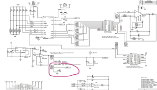
    JMP9 is VREFL. Are you measuring in the right place?

    Best,

    Katlynne Jones

  • Hello Katlynne Jones,

    Thank you for your quick response.

    1. I'm currently using the default settings for JMP1–JMP4 as I'm not fully aware of the required configuration.

    2. The Enable pin is connected to GND, and RST is left open (JMP3 is open).

    3. I'm supplying 3.3V to IOVDD and 5V to AVDD using an external power source.

    4. Apologies for the confusion in my earlier message — I'm actually measuring the output at JMP11.

    Could you please share the recommended configurations for JMP1–JMP4? Also, I’ve attached my SPI timing diagram — could you help verify if it looks correct?

    Thanks & Regards,
    Amara Rakesh

  • Hi Amara, 

    If you want to control the signal through your Arduino, then leave the jumper open. If you are not controlling the signal through the Arduino, then you should close the jumper to ground the signal or leave it open, so the signal is pulled up to IOVDD. You'll need ENABLE and LDAC connected to ground, and RST connected to IOVDD for normal operation. 

    The SPI data you are sending looks correct to load all DAC channels with the data you stored in the temporary registers for each channel. If you haven't previously written any data to the temporary registers, then the outputs will remain at 0V. You can try writing 0x348000.

    Best,

    Katlynne Jones

  • Hi Katlynne Jones,

    Thank you for sharing the 0x348000 command — it worked perfectly for me. I was able to modify the DAC value in the code and successfully observed the corresponding output voltage.

    I have a couple of follow-up questions:

    1. You mentioned, "If you haven't previously written any data to the temporary registers..." — could you please clarify which specific command(s) should be sent prior to using 0x308000?

    2. How can I configure and use a single DAC channel (e.g., only DAC-A) instead of updating all four channels at once?

    3. Currently, I’m using a VREFH of 2.5V. If I want to increase the reference voltage, what is the maximum allowed, and what is the proper way to do so? In that case, should I disable the internal reference and use an external one instead?

    I appreciate your continued support and look forward to your guidance.

    Thanks & Regards,
    Amara Rakesh
  • Hi Amara, 

    Each DAC channel has a temporary (buffer) register and an active register. The command you were doing before was to load the temporary (buffer) register data into the active register which will update the output. If code 0 is in the temporary register (the default) then you are just moving 0 to the active registers which will just set the outputs to 0V. 

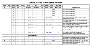
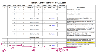
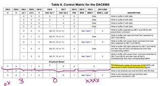
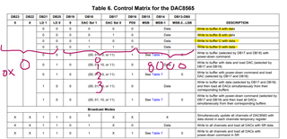
    This command matrix should help you understand which codes to write:

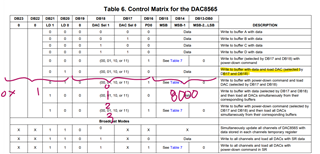
    0x348000 triggers the highlighed command:

    If you want to use 0x30000 to update all outputs with the data from their temporary registers:

    You need to write to each of the temporary registers first with DB18 and DB17 selecting which channel is being written to:

    You can also write to each channel's temporary register and update the output for just that channel at the same time with:

    Maximum reference is determined by this condition: AVDD – (VREFH + VREFL) /2 > 1.2V. Technically the max voltage is AVDD is VREFL is AVDD/2.

    Best,

    Katlynne Jones

  • Hi Katlynne Jones,

    Thank you for explaining everything in such a detailed manner — it was very helpful for me

     Regards,
    Amara Rakesh