ADS131M06-Q1: ads131m02

Part Number: ADS131M06-Q1
Other Parts Discussed in Thread: ADS131M08, ADS131M02, ADS131M06, , ADS124S06, ADS131M04, MSP430FG4619

Tool/software:

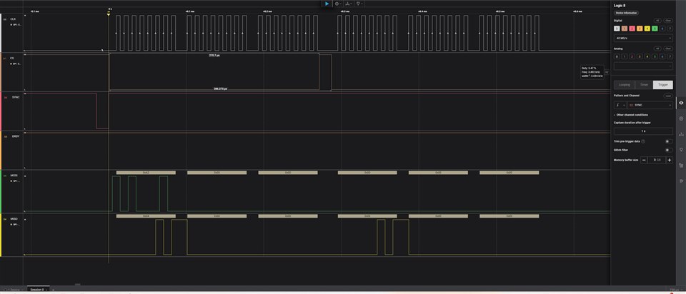
Please see attached scope plots.  we can get the ADS131M02 to work but not he ADS131M08.    

ADS131M08.    DOES NOT WORK

28000 reads analog=0.000 0.000 0.000 0.000 0.000 0.000 volts

first byte returned=28000H=00101000000000000000    is this status register?   What is it saying?


ADS131M02 WORKS

first byte=28180    read analog=0.753   0.753 which are correct voltages

first byte returned=28180H= 00101000000110000000    is this status register?   What is it saying?  Is this reason DRDY stays high?

thanks

  • Hi Peter,

    Are you able to read any register from ADS131M08? Can you provide a clear timing plot like the following timing for data reading or register reading?  In order to read conversion data from ADS131M08, you can send the SPI clocks of 10 words and each word has 24 SCLK clocks.

    Read the GAIN register (0x4 address) with RREG command:


    The answers to your questions:  Yes, the first word is STATUS word, you can check the STATUS Register for the details in the register map in the ADS131M08 datasheet.

    By default, you should be able to see toggling on the /DRDY signal after ADS131M08 is powered up. If you can not see it, please provide your schematic for review.

    BR,

    Dale

  • The returned status value is 24 bits but Table 8-15. STATUS Register Field Descriptions is 15 bits?  Are they padded or is there another Status table I should look at?   We will work on the plots on Monday.  thanks

  • Hi Peter,

    The STATUS register has 16 bits (bit0 - bit15). When the word size is 24 bits, the high 16 bits in the word will be the STATUS data.

    BR,

    Dale

  • Sorry to keep bugging you about ADS131M06 DRDY not changing.  We were able to get the ADS131M02 to work perfectly.  We are sending 8 frames. 

    Attached is schematic of the ADS131 in the bottom left of the attached PDF. Is the wiring incorrect?   Does DRDY require a pull-down resistor?

    DRDY NEVER CHANGES EVEN WHEN DISCONNECTED FROM THE uC after we send the SYNC. DRDY never goes low. We have replaced the ADS131 several times. The ADS Does return data so it is alive. It always returns 1st byte = 280000 so STATUS=CRC change + no new data. DRDY never changes but it returns the 1st byte. Scope plots show CLK right after SYNC but even after long delya, DRDY never changes.

    Keysight scope is not an easy to use logic analyzer. A PC based logic analyzer probably makes more sense. Do you have one that your prefer such as Saleae?

    We have spent Hours trying to make the ADS work. We are tempted to scrap our design and try another A/D.

    ==Is wiring correct?
    ==Does it require Init of registers or reset pins to get DRDY to work?
    ==Is there an easier 6 channel API A/D?

     ADS131schematic.pdf

  • Hi peter,

    Where is your input clock to the ADC (pin 23 - XTAL1/CLKIN)? I could not find it in your schematic, your ADS131M06 symbol does not have this pin 23 and pin 22 (XTAL2). 

    Saleae is a good tool.

    BR,

    Dale

  • We used a Logic analyzer to take these traces.  DRDY is still stuck high. Top trace glitch shows DRDY is connected.  Middle trace reads 6 channels but all are 0.  Bottom trace reads STATUS.  We ignore DRDY since always high, even if we wait long time.  Is ADS SCHEMATIC CORRECT bottom left?  DO WE NEED TO PRESET REGISTERS?

  • Hi peter,

    You did not answer my question, where is your input clock to the ADC (pin 23 - XTAL1/CLKIN)? Your schematic does not show it.

    In your first timing, the /SYNC from your microcontroller was always low, this signal forced the ADC to Reset mode.

    In your second timing, the ADC did not convert as the /SRDY is always high, the clock may be missed.

    In your third timing, your tried to read a register but your SPI configuration on your microcontroller was wrong, your were sending commands to the ADC at the rising edge of SCLK, the right edge is falling edge, the SPI setting should be CPOL = 0 and CPHA = 1.

    BR,

    Dale

  • DaSigmaAdder050325.pdfle,

    Getting a lot closer but the voltages read are completely random (see bottom of screenshot). This is raw output before scaling or negative adjustment. Status register bitmap is always the same so read routine is correct.  .3 volts is on each analog input pin.  Default configuration.  Does schematic look good?  Any ideas why 6 readings are random. thanks

  • ADSCALE_TO_VOLTS 0X6AAAAD //7FFFFF=1.2V = positive full scale 800000h = negative full scale 1/8388607 K/1.2=6990505=0X6AAAAD
    .3 volts seems to read 0x656CC=415436 415436/6990505=.059 when it should be .3
    returned value should be .3 * 6990505 = 2097151 = 0X1FFFFF

    What should returned value be for +.3 volts with default config? 

    ============CORRECTED STATUS INTERPRETATION BELOW=================================================

    status=453F00 analog=7FFFFF 7FFFFF 7B8DD5 68B608 4AEE8B 7FFFFF =synchronization occurred=Reset occured=Ch5 data ok=Ch4 data ok=Ch3 data ok=Ch2 data ok=Ch1 data ok=Ch0 data ok
    status=453F00 analog=5D441A 79595F 415230 FF26AA 7FFFFF F15A07 =synchronization occurred=Reset occured=Ch5 data ok=Ch4 data ok=Ch3 data ok=Ch2 data ok=Ch1 data ok=Ch0 data ok
    status=453F00 analog=63401 6698B 66350 65C12 64C05 642AA =synchronization occurred=Reset occured=Ch5 data ok=Ch4 data ok=Ch3 data ok=Ch2 data ok=Ch1 data ok=Ch0 data ok
    status=453F00 analog=2DAB35 7FFFFF 7FFFFF 7FFFFF BCA42E 15D7D5 =synchronization occurred=Reset occured=Ch5 data ok=Ch4 data ok=Ch3 data ok=Ch2 data ok=Ch1 data ok=Ch0 data ok
    Status bits indicate that Reset or Synchronization may be cause.  Is uC running too slowly?

  • Hi,

    I have noticed you just added an external clock to the XTAL1/CLKIN pin in your latest schematic. Your schematic looks good now, I did not see the REFIN pin of ADS131M06-Q1 in your schematic, I guess it is floating on your real circuit board. 

    You are sending more SCLKs than the SCLKs that is needed for the ADC in one frame. ADS131M06-Q1 requires the SPI clocks for one STATUS word + 6 channel data + one word for CRC = 8 words, you are sending 9 words (each word has 24 SCLKs), so the data on DOUT in the last word (0x053F) in your timing is the right data of the STATUS register, the 3F in 0x053F indicates that the data on all input channels are ready (0x0500 is the default register data).

    You can start the test with internal test signals (shorted input or a DC test signal) by setting MUX[1:0] to a proper value in the CHx_CFG register.

    By default, internal 1.2V Vref is enabled and the gain is 1, so the code for a positive .3V SE input voltage is 

    • 1LSB = (2*1.2/Gain)/2^24 = 0.1430511uV
    • 0.3V/0.143uV=2097152 in decimal = 0x200000 in Hexadecimal format.

    BR,

    Dale

  • After some code fixes, it appears to get a value close to 0X64076 = 409718.  The input on each channel is .3V.  which is off about 5X.  Can you think of a reason why it is not scaled correctly.  I do not change any registers and only use the  wake up value.

  • Hi,

    Can you share a clear timing for a whole frame? I can not see it.

    You raw data from the ADC will be very helpful. 

    How did you generate the signal and connect them to the ADC?

    BR,

    Dale

  • I tried to ground the inputs but it did not correctly read the results.  Please review if the correct register is set to ground the inputs for testing.

    ADS131_writeRegister(0x0, 0x000002);
    ADS131_writeRegister(0x0E, 0x000002);
    ADS131_writeRegister(0x13, 0x000002);
    ADS131_writeRegister(0x18, 0x000002);
    ADS131_writeRegister(0x1D, 0x000002);
    ADS131_writeRegister(0x22, 0x000002);
    for(;;){ FLASHWATCHDOG blinky_stuck=0; ADS131_read(); OS_Delay(ONE_SECOND); } //scale it here but not first status byte

    void ADS131_writeRegister(unsigned int regAddress, unsigned long value24){
    unsigned char cmd1 = 0x40 | (regAddress & 0x1F); // WREG command
    unsigned char cmd2 = 0x00; // write 1 register
    unsigned char byteHigh = (value24 >> 16) & 0xFF;
    unsigned char byteMid = (value24 >> 8) & 0xFF;
    unsigned char byteLow = value24 & 0xFF;
    IO_LOW(P9,BIT7); // Select ADS131
    while (UCB0STAT & UCBUSY);
    SPI_transfer(cmd1);
    SPI_transfer(cmd2);
    SPI_transfer(byteHigh);
    SPI_transfer(byteMid);
    SPI_transfer(byteLow);
    IO_HIGH(P9,BIT7); ; // Deselect ADS131
    }

  • Hi,

    Can you let me know how you ground the input? did you connect both AINxP and AINxN pins to the ground or just just AINxN pin was tied to the ground and then apply a signal to AINxP?

    "ADS131_writeRegister(0x0, 0x000002);" I guess 0x is the register address, are you writing 0x000002 data into the ID register?

    A clear and whole frame will be very helpful to address the issue.

    You can directly read the conversion data without writing or reading any register after the ADC is powered up.

    BR,

    Dale

  • Dale--We tried an off the shelf ADC131M02 and got similar results.  Something must be wrong with the code. We have 0V on one input and .6V on the other input but get strange numbers.  Very simple logic

    INIT SPI         SCAN THE BYTES

     Thanks, Peter

    void ADS131_read(void) { int jj,a; unsigned long res[9]; extern int very_busy; //read all 6 channels into array.
    // Assuming default start up gain=1, 24bit data, and other default conditions so it auto converts.
    // 1LSB = (2*1.2/Gain)/2^24 = 0.1430511uV 0.3V/0.143uV=2097152 in decimal = 0x200000 in Hexadecimal format.
    //10 words are clocked out (response, 8x data, CRC). DIN must be low
    unsigned long byteHigh,byteMid,byteLow;
    SPI_ADS_CONFIG //configure SPI for ADS
    ALL_CS_HI //rstop other tasks
    IO_LOW(P9,BIT4);for(jj=0;jj<10;jj++);IO_HIGH(P9,BIT4); //Sync
    if(P9IN & BIT5){ a=0; while((P9IN & BIT5)&& a++<WAIT4RDY); if(a>(WAIT4RDY-3)) { user_debug_msg("AD NOT READY"); } } //wait for Data Ready to go low
    IO_LOW(P9,BIT7); strTmp[0]=0; // Chip Select ADS13
    for(jj=0;jj<=SCANS;jj++) { //read 7 channels. 1ST WORD IS STATUS
    byteHigh = SPI_transfer(0x00); // Dummy write to read high byte
    byteMid = SPI_transfer(0x00); // Dummy write to read mid byte
    byteLow = SPI_transfer(0x00); // Dummy write to read low byte
    res[jj] = ((unsigned long)byteHigh << 16) + ((unsigned long)byteMid << 8) + (unsigned long)byteLow; // Combine the three bytes into a 24-bit result
    } //read channels
    IO_HIGH(P9,BIT7); ; // no chip select
    sprintf(strTmp, "status=%lX analog=%lX %lX %lX %lX %lX %lX ",res[0],res[1],res[2],res[3],res[4],res[5],res[6]);
    ads131_status_parse(res[0]); //print status
    SPI_FLASH_CONFIG //configure SPI for flash
    }
    /////////////////////// SPI_transfer Transmits one byte over SPI and returns the received byte.
    unsigned int SPI_transfer(unsigned char data) { unsigned char rxbuf;
    while (UCB0STAT & UCBUSY); // Wait for the TX buffer to be ready
    UCB0TXBUF =(unsigned char) data; // Send the byte
    while (UCB0STAT & UCBUSY);// Wait for the RX buffer to receive data
    while (!(IFG2 & UCB0RXIFG)); // Wait for RX complete
    rxbuf=UCB0RXBUF;
    return (rxbuf);// Return the received byte
    }

  • To be sure, all we do is init the SPI ports, then read data.  SPI is used for other circuits on the board with no issues.

    We do not init any registers on the ADS131. 

    Init SPI, then immediately hit Sync and wait for DRDY, then read data. 

    If we need to configure any registers before reading the channels after a reboot, that  would be the problem. thanks

  • Should we try to us an "easier" to implement ADS124S06 instead of the ADS131m06.?  Cannot figure out what we are doing wrong after days of trying.

  • Hi peter,

    ADS131M0x is the easiest ADC to communicate with a microcontroller. As I said, you can directly read the conversion data without writing or reading any register after the ADS131M0x device is powered up.

    My comments were always ignored and my question was ignored as well, these made it more difficult to help you debug.

    For example: As I already said 10 days ago, you were sending more SCLKs than the SCLKs that is needed for the ADC in one frame. The latest timing you shared today has the same problem:

    • This is the first timing you sent to the ADS131M02 ADC, so the first data shifted out by the ADS131M02 ADC to the MISO is 0xFF22, the last 8 bits (0x22) indicates the device ID of ADS131M02. This is a correct response from ADS131M02.
    • ADS131M02 is a 2-ch ADC, so you only need to send 4 words to it (each word is 24-bit length): STATUS word + CH0 data + CH1 data + CRC word. In your timing, you were sending 5 words, so you got 0x0500 on the 5th word as highlighted below, this 0x0500 is actually the data from the STATUS register of the ADC and it should be shown on the first word of next frame if you could follow the correct timing required by the ADC. The timing was messed up here.

    Checking the timing is a direct way to debug as your code actually does not match the timing, but I actually checked the code you shared two days ago and I was confused about "ADS131_writeRegister(0x0, 0x000002);" I guess 0x is the register address and you were writing 0x000002 data into the ID register. I asked but did not get a response yet.

    If you could modify your code and generate a timing like below, I can definitely help you to check, it would be good if you could share your Saleae data file with me so I can check your procedure and also more details. Please note:

    • Below is a timing for 4-ch ADS131M04, you can just send total 4 words for 2-ch ADS131M02. 
    • SPI configuration in you microcontroller should be CPOL=0, CPHA=1. The SPI configuration in your Saleae should be same as well.

    One more thing I would highlight, if you have 0V on one input and .6V on the other input, the differential voltage measured by the ADS131M0x ADC is 0.6V. not 0.3V, so the expected code is:  0.6V/0.143uV=4195804 in decimal = 0x4005DC in Hexadecimal format.

    Thanks&regards,

    Dale

  • Dale, Attached is a re-run along with the setup where .38V is on each input.  We will re-run the 2 channel on Monday.  CPHA = 1  - CPOL = 0 confirmed and checked by ChatGPT.  Thanks for your patience, Peter

  • Session _rename_to_SAL_extension.pdf  your server would not let sal upload so please change extension to SAL for the Salaea scan. thanks

  • Good news is that we used an ADC Click ADS131M02 and it works perfectly and outputs the exact voltage we put into the channels.  Now we will go back to our circuit that uses the ADS131M06.  

  • Hi peter,

    Thanks for update. Why did you always send 5 words (24-bit) to ADS131M02 in one frame?

    -Dale

  • ads131_6channel_380mveachchannel_schematic.pdf

    1 too many scans with M02 but believe this M06 pl

    exampleVoltages.txt
    status=453F00 analog=FFEFD8 FFD622 FFD59D FFE119 FFE839 FFF587 -0.00V -0.00V -0.00V -0.00V -0.00V -0.00V 
    status=453F00 analog=FFEF7E FFD447 FFD8D0 FFE584 FFDC96 30D -0.00V -0.00V -0.00V -0.00V -0.00V 0.00V 
    status=453F00 analog=FFCB4E FFE059 FFC5E0 FFDB02 FFBE0C FFC70E -0.00V -0.00V -0.00V -0.00V -0.00V -0.00V 
    status=453F00 analog=4A5B 4D83 365D 3242 4194 447A 0.00V 0.00V 0.00V 0.00V 0.00V 0.00V 
    status=453F00 analog=47400E CE96C 69C9DC 5CF284 E280EB 509611 0.67V 0.12V 0.99V 0.87V -0.28V 0.76V 
    status=453F00 analog=FFF384 FFF735 FFFCE5 105E FFF175 1E47 -0.00V -0.00V -0.00V 0.00V -0.00V 0.00V 
    status=453F00 analog=278B 1402 25C8 1CCD 2571 1CDB 0.00V 0.00V 0.00V 0.00V 0.00V 0.00V 
    status=453F00 analog=8A998F 86E292 CE4C66 519F0C 8F76F5 28EA97 -1.10V -1.14V -0.47V 0.77V -1.06V 0.38V 
    status=453F00 analog=2982 206E C15 2646 1AA5 FFFECC 0.00V 0.00V 0.00V 0.00V 0.00V -0.00V 
    ot is correct.  All inputs are grounded for tests but this outputs random voltages.  All pins connected.  We have changed ADS131M06.  I and still same results.  Is 12MHz clock a problem?  What can cause random voltages? thanks

  • Hi,

    Is 12MHz you SCLK frequency or mater clock to CLKIN? I would suggest to do an internal short by setting MUX[1:0]=01b and test again.

    -Dale

  • The CLKIN has 8.1MHz but not in sync with SCLK.  I will try MUX[1:0]=01b .  All inputs=0V on this plot. I noticed that some readings are perfect.

  • Hi,

    ADS131M06-Q1 can support SCLK up to 25MHz at 3.3V DVDD.

    - Dale

  • Are you thinking that increasing the SCLK speed to perhaps 16MHz will improve the performance? thanks

  • We put on a 16Mhz clock but it did not fix the problem.  All inputs are grounded.  Some readings are good at uV.  It would appear that the data is shifted to cause an error.

    BAD

    GOOD

  • BAD READUBGS HERE

    There is no obvious reason for the different readings.

  • Can you share the RAW data in excel instead of screenshots? Your status word was incorrect, please share your continuous timings that are captured in logic analyzer so that I can double check.

    -Dale

  • sampling.txt
    status=453F00 analog=27A8 419 309E 1AD0 330C 1522 0.001452V 0.000150V 0.001780V 0.000982V 0.001869V 0.000774V =synchronization occurred=Reset occured=Ch5 data ok=Ch4 data ok=Ch3 data ok=Ch2 data ok=Ch1 data ok=Ch0 data ok
    status=453F00 analog=29E4 3828 184D 3A7D 168F 33BE 0.001534V 0.002057V 0.000890V 0.002142V 0.000826V 0.001895V =synchronization occurred=Reset occured=Ch5 data ok=Ch4 data ok=Ch3 data ok=Ch2 data ok=Ch1 data ok=Ch0 data ok
    status=453F00 analog=3E993 1EA7A 7FFFFF BF79EB 13184D 8C6C56 0.036679V 0.017962V 1.200000V -0.604910V 0.179015V -1.083533V =synchronization occurred=Reset occured=Ch5 data ok=Ch4 data ok=Ch3 data ok=Ch2 data ok=Ch1 data ok=Ch0 data ok
    status=453F00 analog=31EC 2954 11AE 3873 30F2 1365 0.001828V 0.001513V 0.000647V 0.002067V 0.001792V 0.000710V =synchronization occurred=Reset occured=Ch5 data ok=Ch4 data ok=Ch3 data ok=Ch2 data ok=Ch1 data ok=Ch0 data ok
    status=453F00 analog=3894 28DD 3216 1E7B 28FF 3EC9 0.002072V 0.001496V 0.001834V 0.001116V 0.001501V 0.002299V =synchronization occurred=Reset occured=Ch5 data ok=Ch4 data ok=Ch3 data ok=Ch2 data ok=Ch1 data ok=Ch0 data ok
    status=453F00 analog=FFE83F B31 10C FFE461 FFE18D FFE39A -0.000870V 0.000410V 0.000038V -0.001012V -0.001115V -0.001040V =synchronization occurred=Reset occured=Ch5 data ok=Ch4 data ok=Ch3 data ok=Ch2 data ok=Ch1 data ok=Ch0 data ok
    status=453F00 analog=17F5 FFF606 FFFF9A FFF721 26C FFF1D4 0.000877V -0.000365V -0.000015V -0.000325V 0.000089V -0.000519V =synchronization occurred=Reset occured=Ch5 data ok=Ch4 data ok=Ch3 data ok=Ch2 data ok=Ch1 data ok=Ch0 data ok
    status=453F00 analog=D1555A 800000 43F3D2 40EC60 660501 7FFFFF -0.437499V -1.200000V 0.637054V 0.608656V 0.956434V 1.200000V =synchronization occurred=Reset occured=Ch5 data ok=Ch4 data ok=Ch3 data ok=Ch2 data ok=Ch1 data ok=Ch0 data ok
    status=453F00 analog=8979C2 7FFFFF A062D7 800000 74D03 471E26 -1.111166V 1.200000V -0.896381V -1.200000V 0.068445V 0.666729V =synchronization occurred=Reset occured=Ch5 data ok=Ch4 data ok=Ch3 data ok=Ch2 data ok=Ch1 data ok=Ch0 data ok
    status=453F00 analog=45E2DE BCFB98 702EC1 181B83 FAF57C 7FFFFF 0.655183V -0.628287V 1.051712V 0.226008V -0.047260V 1.200000V =synchronization occurred=Reset occured=Ch5 data ok=Ch4 data ok=Ch3 data ok=Ch2 data ok=Ch1 data ok=Ch0 data ok
    status=453F00 analog=207A 2BA7 1CD0 2816 331F 35ED 0.001189V 0.001599V 0.001055V 0.001468V 0.001872V 0.001975V =synchronization occurred=Reset occured=Ch5 data ok=Ch4 data ok=Ch3 data ok=Ch2 data ok=Ch1 data ok=Ch0 data ok
    status=453F00 analog=3AB0 365E 4636 24A1 3FE4 2C37 0.002149V 0.001991V 0.002571V 0.001341V 0.002340V 0.001619V =synchronization occurred=Reset occured=Ch5 data ok=Ch4 data ok=Ch3 data ok=Ch2 data ok=Ch1 data ok=Ch0 data ok
    status=453F00 analog=FFE95F 75E FFF2E6 882 FFF153 FFE3C2 -0.000829V 0.000270V -0.000480V 0.000312V -0.000537V -0.001034V =synchronization occurred=Reset occured=Ch5 data ok=Ch4 data ok=Ch3 data ok=Ch2 data ok=Ch1 data ok=Ch0 data ok
    status=453F00 analog=15E929 890581 4CB05C 7FFFFF 800000 7FFFFF 0.205414V -1.115424V 0.718959V 1.200000V -1.200000V 1.200000V =synchronization occurred=Reset occured=Ch5 data ok=Ch4 data ok=Ch3 data ok=Ch2 data ok=Ch1 data ok=Ch0 data ok
    status=453F00 analog=1824 89E 148F FFFC6F 12C3 21 0.000884V 0.000316V 0.000753V -0.000131V 0.000687V 0.000005V =synchronization occurred=Reset occured=Ch5 data ok=Ch4 data ok=Ch3 data ok=Ch2 data ok=Ch1 data ok=Ch0 data ok
    status=453F00 analog=4BF66A B132BD A4ABA6 EE614C 8CACA 7FFFFF 0.712149V -0.738767V -0.856214V -0.165187V 0.082426V 1.200000V =synchronization occurred=Reset occured=Ch5 data ok=Ch4 data ok=Ch3 data ok=Ch2 data ok=Ch1 data ok=Ch0 data ok
    status=453F00 analog=493425 800000 44E01D 74C566 A80BC4 11882B 0.686285V -1.200000V 0.645707V 1.094729V -0.824569V 0.164362V =synchronization occurred=Reset occured=Ch5 data ok=Ch4 data ok=Ch3 data ok=Ch2 data ok=Ch1 data ok=Ch0 data ok
    status=453F00 analog=4420 3B65 3C15 2920 505F 38CA 0.002495V 0.002175V 0.002200V 0.001506V 0.002943V 0.002080V =synchronization occurred=Reset occured=Ch5 data ok=Ch4 data ok=Ch3 data ok=Ch2 data ok=Ch1 data ok=Ch0 data ok
    3377.digital.csv

    Here are the latest plots using an 8MHz clock.   All inputs are grounded.  Some readings are good and others are wrong.  This web page did not allow me to upload the capture file.  thanks

  • This is a capture file for Saleae.  thanks, peter

  • This is a capture with some perfect and some not perfect data.  they look the same so no idea why it sometimes works.  8Mhz clock looks clean. thanks

  • Hi peter mccormick,

    Thanks for sending the .sal file, that helped.

    In the most recent one I am seeing what looks like all good data, assuming you have the inputs shorted. Either way, both data sets look the same even though the file is named "CaptureGoodandBadReadings". See image below where I converted hex to codes, so these indicate a very small negative voltage being measured

    Can you help explain this discrepancy?

    You are also not reading the complete frame before the next DRDY transition, see the second image below. Can you increase the SCLK speed from 400kHz to at least 1MHz?

    -Bryan

  • I changed the clock to about 1Mhz.  The MSP4304619 appears to be able to keep up with 1MHz.  Attached are captures which do not appear to be as good.captureMay29_131.saldigitalMay29_133.csv

  • Yes, I noticed that DRDY changed before it got to the CRC in frame 8
    I have also seen DRDY change before CRC in some examples you sent for the ADS131M08 or 10 frames total
    I assume it is: Status-6data-crc or 8 frames total

  • The ADS131M02 runs perfectly on this exact same software and reads any voltage + or -.  The only difference is that the ADS131M02 demo board CLKIN is in sync with the SCLK.  Our ADS131M06 uses a 8.2Mhz CLIKIN is not in Sync with SCLK.  I read that it needs to be in sync for precision.  Does the 8.2Mhz CLIKIN need to be in sync with the SCLK?

  • I studied the MIKROE ADC15 https://www.mikroe.com/adc-15-click?srsltid=AfmBOormPq3HM2fr89fdGeZ42l9zzCptcjuqEG5MI0xf-5LSQmT-cpz8 ADS131M02 demo board.  The CLKIN is only 1kHz.  I am surprised that it can operate at this low frequency.  Should we try 1kHz for CLKIN ?

  • Hi peter mccormick,

    As Dale pointed out previously, the DRDY signal is driven high after the last data word is clocked out (but before the CRC word). However, your system is clocking out so slowly that you are actually missing conversions. You can see in the image below that the region I have circled is the region in which you need to clock out data. Your frame (8 words) is much wider than this region, so you are actually still clocking out data when new data is available

    Can you increase the SCLK speed even further? It looks like there are a lot of processing delays between bytes, so I am not sure if you can even speed up the SCLK enough to clock out data within one conversion period. Alternatively you can also slow down the data rate so the conversion period increases. Right now you are at the default of 4kSPS, which gives you 250us to clock out all of the data. Note that at 1MHz it will take 192us (24*8) to clock out all of the data, excluding your processing delays. So you might need to increase SCLK to 10 or 20 MHz, and even then the processing delays might be too significant

    You should not use 1kHz CLK for the ADC. You can see from the Recommended Operating Conditions table 6.3 that the minimum ADC clock is 300 kHz. I don't know why that other board uses a 1kHz clock, but this violates the operating conditions and you should not expect datasheet performance as a result

    -Bryan

  • Thanks for the feedback. We use the antique MSP430FG4619 for 15 years and we have sold thousands. We provide "gateways" which have cellular, satellite, and sensing (www.lasso.com). This Sigma product reads a dozen sensors along with satellite and celluar communication. The MSP430 is swamped doing many tasks and the ADS is only read every few seconds. The MSP does not have time to respond to every DRDY so this may not be a good fit. The SYNC is used to ask the ADS for data when the MSP430 needs data then does other tasks. We may move to the ADS131M04 which we will try tomorrow since we have no trouble with the ADS131M02. I ran the MSP SCLK at 1MHz (attached) and still not good data.
    We also use the TI mmWave for our iRadar which has been a fun product. This ADS has been surprisingly painful to use.
    ==Is the MSP430FG4619 simply not fast enough for the ADS131M06?
    ==The ADS131M02,M04 appears to have the same architecture as the ADS131M06 but easier to use??
    ==TI Documentation seems to show that DRDY goes high before the CRC with no problem.
    ==Can SYNC be used to get data when we need it or do we have to respond to every DRDY?
    We appreciate TIs patience and great support.

    captureMay29_7pm.sal

  • Hi peter mccormick,

    Can you try collecting 4 conversion periods after the SYNC pulse that you generate, instead of 1x?

    In other words, send the SYNC command, then wait for DRDY to go low, clock out data1, wait for DRDY to go low again, clock out data2, etc., until you get 4 complete data frames. Do this with the default ADC settings, and make sure the inputs to the ADC are shorted to ground. This way you are basically reading the ADC noise on each channel

    Alternatively, you can try waiting until the 4th DRDY high to low pulse to clock out data. So, toggle SYNC, then wait for 4 DRDY high to low transitions, then send your SCLKs to collect a single data frame.

    Let me know if the data you get is more consistent. Please take multiple data sets so we can be sure

    -Bryan

  • I will try waiting for the 4th DRDY then take 8 frames (status,6data,crc).  Curious, why would this work better ?

  • Hi peter mccormick,

    The ADS131M06 has a fast startup behavior that outputs unsettled data for the first two conversions after power on, reset, or SYNC. 

    I saw similar behavior on my EVM, where the first few conversions looked unsettled, while I saw settled data every time thereafter. And it did not matter if I used a slower SCLK with a fast data rate that "missed" some DRDY transitions.

    -Bryan

  • You were correct!! :-)  We now don't recognize the reading until the 4th.  I read the mention of fast Startup after SYNC but dismissed it because I did not appreciate how random the data would be. I spent many wasted hours trying to make it work and countless emails to your team. You may want to add to your Docs something like "Take several samples immediately after SYNC startup to allow signals to settle".    Attached are captures if you are curious. Voltages are exact at about .4V on each input.  I think you can close this case.  thanks

  • Hi peter mccormick,

    I would not have expected the errors to be so significant either, which is why we didn't think of this sooner. Also, only seeing the first conversion data obfuscated the issue, because sometimes it was right and sometimes it was wrong (this is the behavior I saw on my EVM as well). Had we looked at multiple conversions in a row, it would have become obvious much sooner

    Glad we could resolve this, thanks for your patience

    -Bryan