


Part Number: AFE2256
Tool/software:
Hello,
I would need clarification about section 7.1.2: Generating Gate Driver Signals from the AFE2256 of the AFE2256 ROIC data sheet.
First, about the SDOUT signal, is the data sheet suggesting the following electrical connections between the ROIC, the FPGA and the Gate Driver?
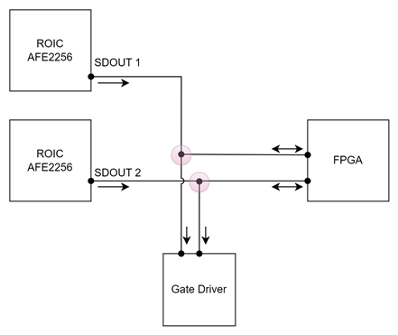
If correct, I see the need to consider isolation between the ROIC/FPGA and Gate Driver junction when having the ROIC communicating to the FPGA on the SDOUT pin..
What's your point of view on this?
Regarding the PROBE GATE DRIVE signal ( PROBE_SIGNAL field value (Register 5Ah), 40h) sent by the AFE2256, I understand it to only be a rising and falling edge.
I understand this rising and falling edge to be used by the FPGA to trigger on the same line signals from the FPGA to the Gate driver, for example: start a line scan, send a clock signal or others
Is that the way it should be working?
Thanks for your inputs on this!