


Part Number: DAC53701
Tool/software:
Hello everyone,
I’m trying to change the address of my I2C device following the pseudocode provided by Katlynne in a response on this forum. After reviewing my implementation, it seems there might be an error in the instructions given.
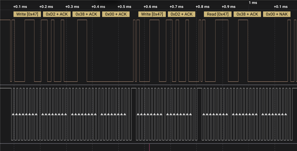
The response mentions that to configure the CONFIG2 register and set GPI_CONFIG to 111b, I should send 0x3100. However, after checking the datasheet, I believe the correct value to send is 0x3800.
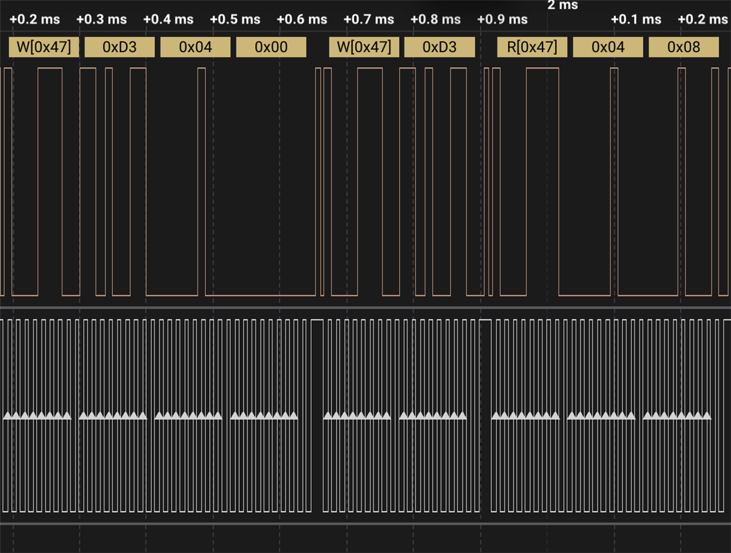
I’ve read back the registers to verify if the data is being written correctly. When I configure GPIO_CONFIG to 0b111 and GPIO_EN to 0b1, I can read them back correctly.
- GPIO_CONFIG to 0b111 writing 0x3100 to the CONFIG2 register (0xD2)
- GPIO_EN to 0b1 writing 0x0400 to the TRIGGER register (0xD3)
However, when I write SLAVE_ADDRESS to 0b01 (0x4000) to the CONFIG2 register (0xD2), reading the register shows it remains at 0.
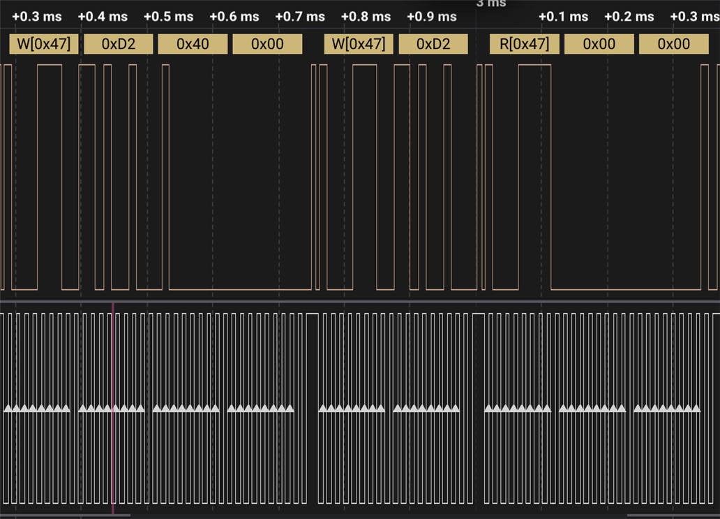
I’m not sure if I’m missing any steps or doing something wrong when attempting to change the address.
Here’s the pseudocode I’m currently using (it’s basically the same as Katlynne’s, but I’ve modified the write to the CONFIG2 register):
#define I2C_ADDR_DAC1 0x48
#define I2C_ADDR_DAC2 0x49
#define I2C_ADDR_BROADCAST 0x47
//Set up I2C address for DAC1 and DAC2
//Set GPI pins to 0 for both devices
//Set GPI_CONFIG in the CONFIG2 register to 111b
Wire.beginTransmission(I2C_ADDR_BROADCAST);
Wire.write(byte(0xD2)); // CONFIG2 Register
Wire.write(byte(0x38)); // Set GPIO_CONFIG to 0b111
Wire.write(byte(0x00)); //
Wire.endTransmission(); // stop transmitting
// Set GPI_EN in the TRIGGER register to 1b
Wire.beginTransmission(I2C_ADDR_BROADCAST);
Wire.write(byte(0xD3)); // TRIGGER Register
Wire.write(byte(0x04)); // Set GPIO_EN to 0b1
Wire.write(byte(0x00)); //
Wire.endTransmission(); // stop transmitting
//Set the GPI pin to logic HIGH for the device that needs to be configured (DAC2)
//Write data to SLAVE_ADDRESS bit field in the CONFIG2 register. Only the device with GPI pin logic HIGH updates the SLAVE_ADDRESS setting passed in the command. Make sure that the rest of the devices on the same I2C bus have their respective GPI pins set to logic LOW during this process.
Wire.beginTransmission(I2C_ADDR_BROADCAST);
Wire.write(byte(0xD2)); // CONFIG2 Register
Wire.write(byte(0x40)); // Set SLAVE_ADDRESS to 0b01
Wire.write(byte(0x00)); //
Wire.endTransmission(); // stop transmitting
//Toggle the GPI pin of the device bring programmed to logic LOW
//Set GPI_EN to 0b
Wire.beginTransmission(I2C_ADDR_BROADCAST);
Wire.write(byte(0xD3)); // TRIGGER Register
Wire.write(byte(0x00)); // Set GPIO_EN to 0b0
Wire.write(byte(0x00)); //
Wire.endTransmission(); // stop transmitting
// Change GPI_CONFIG to 000b
Wire.beginTransmission(I2C_ADDR_BROADCAST);
Wire.write(byte(0xD2)); // CONFIG2 Register
Wire.write(byte(0x00)); // Set GPIO_CONFIG to 0b000
Wire.write(byte(0x00)); //
Wire.endTransmission(); // stop transmitting
//Trigger NVM write operation.
Wire.beginTransmission(I2C_ADDR_BROADCAST);
Wire.write(byte(0xD3)); // TRIGGER Register
Wire.write(byte(0x00)); //
Wire.write(byte(0x10)); // Set NVM_PROG to 0b1
Wire.endTransmission(); // stop transmitting
//Power-up DAC1, enable VDD reference, SLEW_RATE: 1.6384 ms (Square wave frequency: 610 Hz)
Wire.beginTransmission(I2C_ADDR_DAC1);
Wire.write(byte(0xD1)); // GENERAL_CONFIG Register
Wire.write(byte(0xC1)); //
Wire.write(byte(0x00)); //
Wire.endTransmission(); // stop transmitting
//Set MARGIN_HIGH on DAC1
Wire.beginTransmission(I2C_ADDR_DAC1);
Wire.write(byte(0x25)); // DAC_MARGIN_HIGH Register
Wire.write(byte(0x0F)); //
Wire.write(byte(0xFC)); //
Wire.endTransmission(); // stop transmitting
//Set MARGIN_LOW on DAC1
Wire.beginTransmission(I2C_ADDR_DAC1);
Wire.write(byte(0x26)); // DAC_MARGIN_LOW Register
Wire.write(byte(0x00)); //
Wire.write(byte(0x00)); //
Wire.endTransmission(); // stop transmitting
//Set DAC1 GPIO to trigger square wave
Wire.beginTransmission(I2C_ADDR_DAC1);
Wire.write(byte(0xD2)); // CONFIG2 Register
Wire.write(byte(0x18)); // Set GPIO_CONFIG to 0b011
Wire.write(byte(0x00)); //
Wire.endTransmission(); // stop transmitting
//Power-up DAC2, enable VDD reference
//CODE_STEP: 8 LSB, SLEW_RATE: 204.8 µs x 1.75 = 358.4 µs (Envelope rise/fall times for full-scale:~26 ms)
Wire.beginTransmission(I2C_ADDR_DAC2);
Wire.write(byte(0xD1)); // GENERAL_CONFIG Register
Wire.write(byte(0x0A)); //
Wire.write(byte(0x80)); //
Wire.endTransmission(); // stop transmitting
//OPTION-3: Configure DAC2 GPIO to trigger high-priority alarm with minimum time settings and trigger
Wire.beginTransmission(I2C_ADDR_DAC2);
Wire.write(byte(0xD2)); // CONFIG2 Register
Wire.write(byte(0x20)); // Set GPIO_CONFIG to 0b100
Wire.write(byte(0x00)); //
Wire.endTransmission(); // stop transmitting
//Set MARGIN_HIGH on DAC2
Wire.beginTransmission(I2C_ADDR_DAC2);
Wire.write(byte(0x25)); // DAC_MARGIN_HIGH Register
Wire.write(byte(0x0F)); //
Wire.write(byte(0xFC)); //
Wire.endTransmission(); // stop transmitting
//Set MARGIN_LOW on DAC2
Wire.beginTransmission(I2C_ADDR_DAC2);
Wire.write(byte(0x26)); // DAC_MARGIN_LOW Register
Wire.write(byte(0x00)); //
Wire.write(byte(0x00)); //
Wire.endTransmission(); // stop transmitting
// Set GPI_EN in the TRIGGER register to 1b
Wire.beginTransmission(I2C_ADDR_BROADCAST);
Wire.write(byte(0xD3)); // TRIGGER Register
Wire.write(byte(0x04)); // Set GPIO_EN to 0b1
Wire.write(byte(0x00)); //
Wire.endTransmission(); // stop transmitting
//Trigger NVM write operation.
Wire.beginTransmission(I2C_ADDR_BROADCAST);
Wire.write(byte(0xD3)); // TRIGGER Register
Wire.write(byte(0x00)); //
Wire.write(byte(0x10)); // Set NVM_PROG to 0b1
Wire.endTransmission(); // stop transmitting

